Page 345 - Organic Electronics in Sensors and Biotechnology
P. 345

322    Cha pte r  Ei g h t

               traps.  Likewise, in the studies of photoresponse, an observation of
                    110
               high responsivity R, which is defined as J /P, where J  is the photo-
                                                  ph         ph
               current density (total drain current I upon illumination minus the
                                               d
               dark current per unit area) and P is the illumination power density,
                                                                       101
               can be affected by electron trapping at the interface near the gate
                            96
               dielectric layer  and the electrode work function.  From the applica-
                                                        98
               tion side, a distinct feature of the light-sensing properties of OFETs is
               that R can be tuned by orders of magnitude by an applied V . The
                                                                    g
               largest measured R values are on the order of 1 to 100 A/W among all
               organic devices prepared by Narayan and Kumar on single-layer poly
                          90
               P3HT OFETs  and by Noh et al. on single-layer 2,5-dibromothieno
                                    101
                                                       111
               [3,2-b]thiophene (BPTT).  A photovoltaic effect and high R 112, 113  are
               reported on ambipolar transistors based on a bulk heterojunction
               concept. Such a highly photoresponsive OFET based on photoin-
               duced charge transfer layer of C  and ZnPc mixed layer as a photoac-
                                          60
               tive layer is shown in Fig. 8.17. In this experiment, using a mask to
               illuminate only the active channel of the OFET with minimized arti-
                                      1
               facts, a large R of 10  to 10  A/W depending on the intensity of illu-
                                −3
               mination and on applied V  could be obtained. 114
                                      g
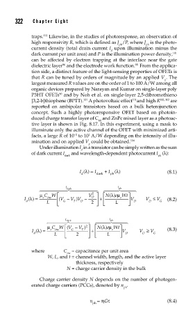
                   Under illumination I  in a transistor can be simply written as the sum
                                   d
               of dark current I   and wavelength-dependent photocurrent I  (λ):
                            dark                                 ph
                                     λ
                                   I () =  I  +  I ()                (8.1)
                                                 λ
                                   d     dark  ph
                                                  I


                   	         I dark
                                                  ph
                   μ  CW ⎡             2  ⎤  ⎡N()λμ   ⎤
                                                 e Wt
             I () =  e  ins  ( ⎢  V −  V V −  V D  ⎥ + ⎢  e  ⎥ V  V ≤ V  (8.2)
                                                               ≤
               λ
                                 )
             d       L      G   T  D   2    ⎣    L    ⎦  D    D   G
                          ⎣              ⎦


                      	      I 
         	    I
                                               ph
                             dark
                             ( ⎡
                      μ  CW V −   V ) ⎤  ⎡N()λμ   ⎤
                                     2
                                             e Wt
                  λ
                I () =  e  ins  ⎢  G  T  ⎥ + ⎢  e  ⎥ V    V  ≥ V     (8.3)
                d       L        2       ⎣   L    ⎦  D     D    G
                             ⎣        ⎦
               where        C  = capacitance per unit area
                             ins
                      W, L, and t =  channel width, length, and the active layer
                                 thickness, respectively
                             N = charge carrier density in the bulk
                   Charge carrier density N depends on the number of photogen-
               erated charge carriers (PCCs), denoted by n .
                                                    ph
                                       n =η Gτ                       (8.4)
                                        ph
   340   341   342   343   344   345   346   347   348   349   350