Page 344 - Organic Electronics in Sensors and Biotechnology
P. 344

Organic Electronics in Memories and Sensing Applications   321


                                            Light (top)

                              x
                                    S                        D


                                    Au                       Au
                              t
                              d
                                            C 60 + ZnPc

                     Interface                  BCB
                      x = 0
                                      ITO


                                                 G


                                              Light (bottom)

                         10 –5
                         10 –6
                                 –5
                                10    2.2 mW; through ITO
                         10 –7        2.9 mW; through ITO
                                      3.7 mW; through ITO
                                      3.7 mW; through Au
                        I d  (A)  10 –8  Drain current (A)  10 –6   2.9 mW; through Au
                                      2.2 mW; through
                                         Au
                                                          2.9 mW;  780 nm
                         10 –9             λ =  780 nm    2.2 mW; 780 nm
                                  –60  –30  0  30  60     3.7 mW; 780 nm
                                      Gate voltage (V)   Dark
                        10 –10                           21 μW; 530 nm
                                                         66 μW; 530 nm
                                                         110 μW; 530 nm
                        10 –11
                            –60   –40   –20    0     20    40     60
                                              V g  (V)
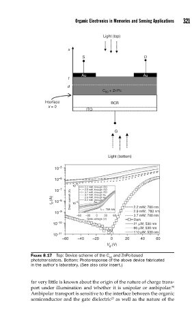
               FIGURE 8.17  Top: Device scheme of the C  and ZnPc-based
                                               60
               phototransistors. Bottom: Photoresponse of the above device fabricated
               in the author’s laboratory. (See also color insert.)

               far very little is known about the origin of the nature of charge trans-
                                                                        90
               port under illumination and whether it is unipolar or ambipolar.
               Ambipolar transport is sensitive to the interface between the organic
               semiconductor and the gate dielectric  as well as the nature of the
                                                23
   339   340   341   342   343   344   345   346   347   348   349