Page 339 - Organic Electronics in Sensors and Biotechnology
P. 339

316    Cha pte r  Ei g h t


               10 –4                         10 –4
                      V = –30 V                      V =  –30 V
                                                      d
                       d
               10 –5                         10 –5
                          Programming          –6      Programming
                –6
             (A)  10       (V  = 200 V)     (A)  10     V  = –200 V
                            g
                                                         g
             –I d  10 –7  1 st  Erasing     –I d  10 –7  1 st
               10 –8  nd    (V  = –100 V)    10 –8   nd    Erasing
                             g
                     2                              2     V  = –200 V
                                                           g
               10 –9  3 rd                   10 –9  3 rd
                   –40 –20 0  20 40 60 80       –150  –100   –50    0
                           V (V)                           V (V)
                            g
                                                            g
                             (a)                            (b)
             V g Prog.  (V)  200             10 –5   V =  –10 V
                                                      d
                                               –6
              100
                                             10
                                                       Programming
                0
                                                          g
             –100                           (A)  10 –7  1 st  V  = 60 V
                                                           Erasing
                                               –8
             (A) 10 –3                      –I d  10 –9  2 nd  V  = –50 V
                                                            g
                                                     rd
                                             10
                                                    3
                –5
             –I d 10                                4 th
              10 –7                                 5 th
                  0  20   40  60  80  100        –20  –10   0   10   20
                          Time (μs)                        V (V)
                                                            g
                             (c)                            (d)
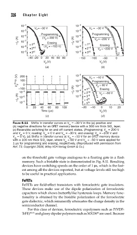
          FIGURE 8.11  Shifts in transfer curves at V  = –30 V in the (a) positive and
                                          ds
          (b) negative directions for an OFET memory device with a 300 nm thick SiO  layer.
                                                                  2
          (c) Reversible switching for on and off current states. (Programming: V  = 200 V
                                                              gs
          and V  = 0 V, reading: V  = 0 V and V  = –30 V, and erasing: V  = –100 V and
              ds            gs        ds                 gs
          V  = 0 V). (d) Shifts in transfer curves at V  = –10 V for an OFET memory device
           ds                             ds
          with a 100 nm thick SiO  layer, where V  = 60 V and V  = –50 V were applied for
                            2           gs         gs
          1 μs for programming and erasing, respectively. (Reproduced with permission from
          Ref. 73. Copyright 2006, Wiley VCH Verlag GmbH & Co.)
               on the threshold gate voltage analogous to a floating gate in a flash
               memory. Such a bistable state is demonstrated in Fig. 8.11. Resulting
               devices have switching speeds on the order of 1 μs, which is the fast-
               est among all the devices reported, but at voltage levels still too high
               to be useful in practical applications.
               FeFETs
               FeFETs are field-effect transistors with ferroelectric gate insulators.
               These devices make use of the dipole polarization of ferroelectric
               capacitors which shows butterflylike hysteresis loops. Memory func-
               tionality is obtained by the bistable polarization of the ferroelectric
               gate dielectric, which remanently attenuates the charge density in the
               semiconductor channel.
                   For this class of devices, ferroelectric copolymers such as P(VDF-
               TrFE) 80, 81  and glassy dipolar polymers such as MXD6  are used. Because
                                                          82
   334   335   336   337   338   339   340   341   342   343   344