Page 338 - Organic Electronics in Sensors and Biotechnology
P. 338

Organic Electronics in Memories and Sensing Applications   315


                                             g
                                       10 –6  V  = 10 V  V drain  = 15 V  40
                                      I drain  (μA)  10 –7
                                              5 V
               10 –6                         2 V                 V Gate  (V)
                                            0 V                    20
                                       10 –8
                                          0      250    500
             I drain  (μA)  10 –7                  Time (s)        0    V gate  (V)

                                  V drain  = 15 V

               10 –8
                                                 Memory window     –20
                                                 after 1000 s


               10 –9
                       0       200     400      600     800      1000
                                        Time (s)
                                          (a)

               10 –6
                                                    V    = 15 V
                                 “Writing”           drain
                                                                    10

               10 –7


            I drain (A)  10 –8                   “On”                0   V gate  (V)

                        “Off”
                                                           “Erased”

               10 –9

                                                                    –10

               10 –10
                   0          50          100         150         200
                                         Time (s)
                                          (b)
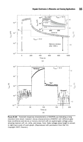
          FIGURE 8.10  Transient response characteristics of BiOFETs (a) indicating a long
          retention time (inset: transient decay characteristics of BiOFET with different gate
          bias conditions) and (b) as a memory element with an applied gate voltage pulse
          showing memory off, on, write, and erase. Note: Gate voltage pulse height is shown
          in right-hand scale of each graph. (Reproduced with permission from Ref. 53.
          Copyright 2007, Elsevier.)
   333   334   335   336   337   338   339   340   341   342   343