
Page 341 - Organic Electronics in Sensors and Biotechnology
P. 341
318 Cha pte r Ei g h t
100
75
50
25
0
–25
–50
–75 (a)
100
75
50
(mC/m 2 ) 25 0
D –25
–50
–75 (b)
100
75
50
25
0
–25
–50
–75 (c)
–100
–180 –120 –60 0 60 120 180
–E (MV/m)
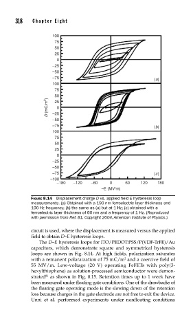
FIGURE 8.14 Displacement charge D vs. applied fi eld E hysteresis loop
measurements. (a) Obtained with a 190 nm ferroelectric layer thickness and
100 Hz frequency; (b) the same as (a) but at 1 Hz; (c) obtained with a
ferroelectric layer thickness of 60 nm and a frequency of 1 Hz. (Reproduced
with permission from Ref. 81. Copyright 2004, American Institute of Physics.)
circuit is used, where the displacement is measured versus the applied
field to obtain D–E hysteresis loops.
The D–E hysteresis loops for ITO/PEDOT:PSS/P(VDF-TrFE)/Au
capacitors, which demonstrate square and symmetrical hysteresis
loops are shown in Fig. 8.14. At high fields, polarization saturates
with a remanent polaraization of 75 mC/m and a coercive field of
2
55 MV/m. Low-voltage (20 V) operating FeFETs with poly(3-
hexylthiophene) as solution-processed semiconductor were demon-
strated as shown in Fig. 8.15. Retention times up to 1 week have
81
been measured under floating gate conditions. One of the drawbacks of
the floating gate operating mode is the slowing down of the retention
loss because charges in the gate electrode are not free to exit the device.
Unni et al. performed experiments under nonfloating conditions