
Page 342 - Organic Electronics in Sensors and Biotechnology
P. 342
Organic Electronics in Memories and Sensing Applications 319
On
10 –8 V D = –10 mV 200
190
L = 15 μm 180
W = 6 mm On/off ratio 170
160
–I D (A) 10 –9 150
140
130
100
Time (min)
10 –10
Off
0 50 100 150 200
Time (min)
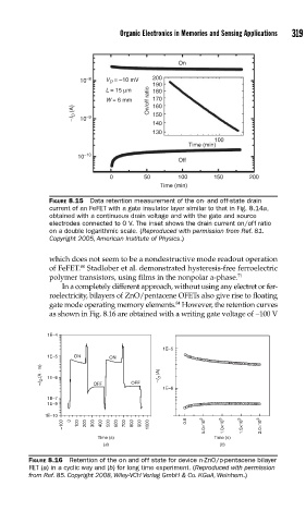
FIGURE 8.15 Data retention measurement of the on- and off-state drain
current of an FeFET with a gate insulator layer similar to that in Fig. 8.14a,
obtained with a continuous drain voltage and with the gate and source
electrodes connected to 0 V. The inset shows the drain current on/off ratio
on a double logarithmic scale. (Reproduced with permission from Ref. 81.
Copyright 2005, American Institute of Physics.)
which does not seem to be a nondestructive mode readout operation
80
of FeFET. Stadlober et al. demonstrated hysteresis-free ferroelectric
71
polymer transistors, using films in the nonpolar a-phase.
In a completely different approach, without using any electret or fer-
roelectricity, bilayers of ZnO/pentacene OFETs also give rise to floating
84
gate mode operating memory elements. However, the retention curves
as shown in Fig. 8.16 are obtained with a writing gate voltage of −100 V
1E–4
1E–5
1E–5 ON ON
–I D (A · m) 1E–6 –I D (A)
OFF
OFF
1E–6
1E–7
1E–9
1E–10
–100 0 100 200 300 400 500 600 700 800 900 1000 0.0 5.0×10 2 1.0×10 3 1.5×10 3 2.0×10 3
Time (s) Time (s)
(a) (b)
FIGURE 8.16 Retention of the on and off state for device n-ZnO/p-pentacene bilayer
FET (a) in a cyclic way and (b) for long time experiment. (Reproduced with permission
from Ref. 85. Copyright 2008, Wiley-VCH Verlag GmbH & Co. KGaA, Weinhem.)