Page 346 - Organic Electronics in Sensors and Biotechnology
P. 346
Organic Electronics in Memories and Sensing Applications   323

               which depends on the quantum efficiency for charge carrier genera-
               tion η, the generation rate G, and the average lifetime of the PCC τ.
                   The generation rate G is given by the product of absorption coef-
               ficient α(λ) and the photon flux density φ per unit area per unit time.
               If we assume that charge generation takes place within the active
               region, i.e., η≠ 0 for 0 ≤ x ≤ d and η = 0 for d ≤ x ≤ t and I  (λ) is pri-
                                                               ph
               marily controlled by the generation process in the regime above the
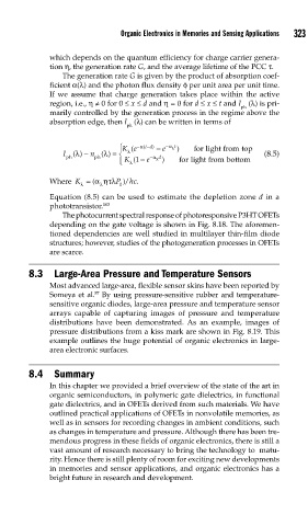
               absorption edge, then I  (λ) can be written in terms of
                                   ph

                                        −
                                 ⎧ ⎪ Ke − α (  td)  −  e − α λ t  )  for light frrom top
                                    (
                      λ
                             λ
                   I () ∼  n () = ⎨  λ                               (8.5)
                    ph     ph     K (1 −  e − α λ )  for light from bottom
                                           d
                                 ⎩ ⎩ ⎪  λ
               Where  K = ( αητλ P )/ hc.
                            λ
                       λ
                                 0
               Equation (8.5) can be used to estimate the depletion zone d in a
               phototransistor. 103
                   The photocurrent spectral response of photoresponsive P3HT OFETs
               depending on the gate voltage is shown in Fig. 8.18. The aforemen-
               tioned dependencies are well studied in multilayer thin-film diode
               structures; however, studies of the photogeneration processes in OFETs
               are scarce.
          8.3  Large-Area Pressure and Temperature Sensors
               Most advanced large-area, flexible sensor skins have been reported by
                           57
               Someya et al.  By using pressure-sensitive rubber and temperature-
               sensitive organic diodes, large-area pressure and temperature sensor
               arrays capable of capturing images of pressure and temperature
               distributions have been demonstrated.  As an example, images of
               pressure distributions from a kiss mark are shown in Fig. 8.19. This
               example outlines the huge potential of organic electronics in large-
               area electronic surfaces.


          8.4 Summary
               In this chapter we provided a brief overview of the state of the art in
               organic semiconductors, in polymeric gate dielectrics, in functional
               gate dielectrics, and in OFETs derived from such materials. We have
               outlined practical applications of OFETs in nonvolatile memories, as
               well as in sensors for recording changes in ambient conditions, such
               as changes in temperature and pressure. Although there has been tre-
               mendous progress in these fields of organic electronics, there is still a
               vast amount of research necessary to bring the technology to  matu-
               rity. Hence there is still plenty of room for exciting new developments
               in memories and sensor applications, and organic electronics has a
               bright future in research and development.

