
Page 337 - Organic Electronics in Sensors and Biotechnology
P. 337
314 Cha pte r Ei g h t
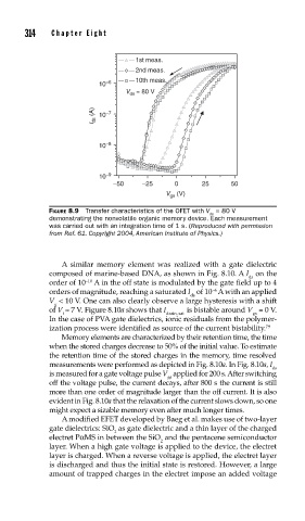
1st meas.
2nd meas.
10th meas.
10 –6
V ds = 80 V
I ds (A) 10 –7
10 –8
10 –9
–50 –25 0 25 50
V (V)
gs
FIGURE 8.9 Transfer characteristics of the OFET with V = 80 V
ds
demonstrating the nonvolatile organic memory device. Each measurement
was carried out with an integration time of 1 s. (Reproduced with permission
from Ref. 61. Copyright 2004, American Institute of Physics.)
A similar memory element was realized with a gate dielectric
composed of marine-based DNA, as shown in Fig. 8.10. A I on the
ds
order of 10 A in the off state is modulated by the gate field up to 4
−10
orders of magnitude, reaching a saturated I of 10 A with an applied
−6
ds
V < 10 V. One can also clearly observe a large hysteresis with a shift
g
of V ≈ 7 V. Figure 8.10a shows that I is bistable around V = 0 V.
t drain, sat gs
In the case of PVA gate dielectrics, ionic residuals from the polymer-
ization process were identified as source of the current bistability. 79
Memory elements are characterized by their retention time, the time
when the stored charges decrease to 50% of the initial value. To estimate
the retention time of the stored charges in the memory, time resolved
measurements were performed as depicted in Fig. 8.10a. In Fig. 8.10a, I
ds
is measured for a gate voltage pulse V applied for 200 s. After switching
gs
off the voltage pulse, the current decays, after 800 s the current is still
more than one order of magnitude larger than the off current. It is also
evident in Fig. 8.10a that the relaxation of the current slows down, so one
might expect a sizable memory even after much longer times.
A modified EFET developed by Baeg et al. makes use of two-layer
gate dielectrics: SiO as gate dielectric and a thin layer of the charged
2
electret PαMS in between the SiO and the pentacene semiconductor
2
layer. When a high gate voltage is applied to the device, the electret
layer is charged. When a reverse voltage is applied, the electret layer
is discharged and thus the initial state is restored. However, a large
amount of trapped charges in the electret impose an added voltage