
Page 335 - Organic Electronics in Sensors and Biotechnology
P. 335
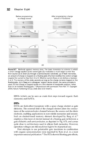
312    Cha pte r  Ei g h t


                 Before programming;             After programming; charge
                   no charge stored                 stored in FG/electret
                       G

                       FG                              +++++++
             S                    D
                      Closed
                                                         Open
            Semiconductor substrate
                                        (a)

             S                    D

                      Closed
                                                         Open
            Semiconductor layer
                      Electret                        ++++++++++
                        G
                                        (b)

          FIGURE 8.7  Methods against memory loss. The basic transistor is a device in which
          a small voltage applied at the control gate (G) modulates a much larger current fl ow
          from source (S) to drain (D) through a semiconductor substrate. (a) In fl ash memories,
          an amount of charge is trapped on a fl oating gate (FG) that modifi es the control voltage
          required for current to fl ow from S to D. Whether current fl ows or not defi nes a boolean
          1 or 0. The memory of this state persists as long as the charge remains trapped on the
          fl oating gate. (b) In Baeg and colleagues’ organic device shown, the same principle is
          used, but the charge is trapped locally on a thin electret of chargeable polymer, rather
                                  73
          than on an isolated fl oating gate.  (Reproduced with permission from Ref. 77. Copyright
          2004, Nature Publishing Group.) (See also color insert.)


               EFETs (which can be seen as crude first steps toward organic flash
               elements) and FeFETs.

               EFETs
               EFETs are field-effect transistors with a space charge electret as gate
               dielectric. The external field of the charged electret alters the conduc-
               tance of the semiconductor channel between the source and the drain
               electrode, enabling applications in nonvolatile memories and sensors.
                                                                        73
               Such an electret-based memory element developed by Baeg et al.
               employs a thin layer of electret instead of a floating gate in between a
               gate dielectric and semiconductor, as depicted in Fig. 8.7b, and comes
               quite close to architectures used in silicon flash memories. However,
               operation voltages are still much too high to be of practical use.
                   First attempts to use polarizable gate insulators in combination
               with organic semiconductors were reported by Katz et al. in a most
                                         78
               important seminal publication.  The FETs showed floating gate effects,