
Page 336 - Organic Electronics in Sensors and Biotechnology
P. 336
Organic Electronics in Memories and Sensing Applications 313
S D
Semiconductor
– – – – – – – –
Space charge electret
G
+ + + + + + +
Conductive substrate
S D
Semiconductor
G Dipolar electret
Conductive substrate
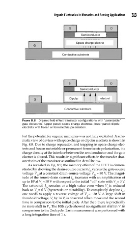
FIGURE 8.8 Organic fi eld-effect transistor confi gurations with “polarizable”
gate dielectrics. Upper panel: space charge electrets; lower panel: dipole
electrets with frozen or ferroelectric polarization.
but the potential for organic memories was not fully exploited. A sche-
matic view of devices with space charge or dipolar electrets is shown in
Fig. 8.8. Due to charge separation and trapping in space charge elec-
trets and frozen metastable or permanent ferroelectric polarization, the
charge density at the interface between the semiconductor and the gate
electret is altered. This results in significant effects in the transfer char-
acteristics of the transistor as outlined in detail below.
As revealed in Fig. 8.9, the memory effect of the EFET is demon-
strated by showing the drain-source current I versus the gate-source
ds
voltage V at a constant drain-source voltage V = 80 V. The magni-
gs ds
tude of the source-drain current I increases with an amplification of
ds
up to 10 at V ≈ 50 V with respect to the initial “off” state with V = 0 V.
4
g g
The saturated I remains at a high value even when V is reduced
ds g
back to V = 0 V (hysteresis or bistability). To completely deplete I ,
g ds
one needs to apply a reverse voltage of V ≈ −30 V. A large shift in
g
threshold voltage, V by 14 V, is observed when measured the second
t
time in comparison to the initial cycle. After that, there is practically
no more shift in V . The 10th cycle showed no significant shift in V in
t t
comparison to the 2ndcycle. Each measurement was performed with
a long integration time of 1 s.