
Page 91 - Organic Electronics in Sensors and Biotechnology
P. 91
68 Cha pte r T w o
The devices were tested as p-channel materials with an Agilent
4155 C semiconductor parameter analyzer kept in a glove box at room
temperature. The field-effect mobilities in saturation regimes were
extracted using the well-known equation 59
2
I = C μ (W/2L) (V − V ) at V > V (2.2)
ds i g t ds g
where I = drain-source current
ds
C = capacitance per unit area of the gate dielectric layer
i
V = gate voltage
g
V = threshold voltage
t
1/2
Voltage V was extrapolated from the (I ) vs. V plot.
t ds g
−3
2
Channel mobilities as high as 1.6 × 10 cm /(V⋅ s) with an on/off
4
ratio of 2 × 10 were reached with a bottom-contact geometry. These
figures were slightly improved by annealing the substrate film for
2
−3
30 min at 100°C, resulting in a mobility of 2.8 × 10 cm /(V⋅ s) and an
on/off ratio of 6 × 10 . Postthermal annealing treatments have been
4
known to improve molecular ordering and grain sizes of the thin film
and frequently result in better device performance. Moreover, anneal-
ing may reduce also the concentration of adsorbed impurity dopants
(moisture and oxygen), increasing the OTFT properties. 128–130
Field-effect mobility greater than one order of magnitude was
achieved for spin-coated and annealed top-contact OTFT. Top-
contact devices were fabricated using a highly n-doped silicon wafer
(resistivity 20 Ω ⋅ cm) as gate contact on which 100 nm of dielectric
(SiO ) was thermally grown. Gold was used as the source and drain
2
electrodes, and it was deposited on organic active layer through a
shadow mask with a channel width (W) of 500, 1000, 2000, and 4000 μm
and a channel length of 150, 100, 100, and 200 μm, respectively.
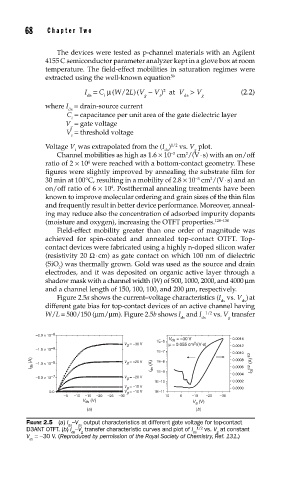
Figure 2.5a shows the current–voltage characteristics (I vs. V )at
ds ds
different gate bias for top-contact devices of an active channel having
W/L = 500/150 (μm/μm). Figure 2.5b shows I and I 1/2 vs. V transfer
ds ds g
–2.0 × 10 –6
V ds = –30 V 0.0014
1E–6
V g = –30 V μ = 0.055 cm 2 /(V . s)
–1.5 × 10 –6 0.0012
1E–7 0.0010
I ds (A) –1.0 × 10 –6 V g = –25 V I ds (A) 1E–8 0.0008 I ds 1/2 (A) 1/2
0.0006
1E–9
0.0004
–5.0 × 10 –7 V g = –20 V
1E–10 0.0002
V g = –15 V
0.0000
0.0 V g = –10 V 1E–11
–5 –10 –15 –20 –25 –30 10 0 –10 –20 –30
V ds (V) V g (V)
(a) (b)
FIGURE 2.5 (a) I –V output characteristics at different gate voltage for top-contact
ds ds
D3ANT OTFT. (b) I –V transfer characteristic curves and plot of I ds 1/2 vs. V at constant
g
g
ds
V =−30 V. (Reproduced by permission of the Royal Society of Chemistry, Ref. 131.)
ds