
Page 92 - Organic Electronics in Sensors and Biotechnology
P. 92
Or ganic Thin-Film Transistors for Inor ganic Substance Monitoring 69
characteristics at source-drain voltage fixed at −30 V. Such plots show
that D3ANT-based OTFT exhibits a well shaped p-channel response,
with defined linear and saturation regions. An averaged mobility of
2
−2
1.3 × 10 cm /(V⋅ s) was observed with on/off ratio varying from 10 to
3
2
5
10 . The highest mobility reached was 0.055 cm /(V⋅ s) while optimized
on/off ratios reached the value of 4 × 10 . Data reported in Fig. 2.5 are
5 131
relevant to the best mobility device (spin and annealed film). The
−2
observed mobilities of ~10 cm /(V ⋅ s) are the highest reported so far
2
for solution processed anthracene oligomers. 132–133
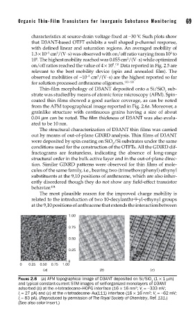
Thin-film morphology of D3ANT deposited onto a Si/SiO sub-
2
strate was studied by means of atomic force microscopy (AFM). Spin-
coated thin films showed a good surface coverage, as can be noted
from the AFM topographical image reported in Fig. 2.6a. Moreover, a
grainlike structure with continuous grains having a size of about
0.04 μm can be noted. The film thickness of D3ANT was also evalu-
ated to be 10 nm.
The structural characterization of D3ANT thin films was carried
out by means of out-of-plane GIXRD analysis. Thin films of D3ANT
were deposited by spin coating on SiO /Si substrates under the same
2
conditions used for the construction of the OTFTs. All the GIXRD dif-
fractograms are featureless, indicating the absence of long-range
structural order in the bulk active layer and in the out-of-plane direc-
tion. Similar GIXRD patterns were observed for thin films of mole-
cules of the same family, i.e., bearing two (trimethoxyphenyl) ethynyl
substituents at the 9,10 positions of anthracene, which are also inher-
ently disordered though they do not show any field-effect transistor
behavior. 134
The most plausible reason for the improved charge mobility is
related to the introduction of two 10-decylanthr-9-yl-ethynyl groups
at the 9,10 positions of anthracene that extends the interaction between
1.00
0.75
0.50
0.25
0
0 0.25 0.50 0.75 1.00
(a) (b) (c)
FIGURE 2.6 (a) AFM topographical image of D3ANT deposited on Si/SiO (1 × 1 μm)
2
and typical constant-current STM images of self-organized monolayers of D3ANT
adsorbed (b) at the n-tetradecane–HOPG interface (16 × 16 nm ; V =−333 mV;
2
t
2
I = 27 pA) and (c) at the n-tetradecane–Au(111) interface (16 × 16 nm ; V =−62 mV;
t t
I = 83 pA). (Reproduced by permission of The Royal Society of Chemistry, Ref. 131.)
t
(See also color insert.)