Page 213 - Phase-Locked Loops Design, Simulation, and Applications
P. 213
MIXED-SIGNAL PLL APPLICATIONS PART 1: INTEGER-N FREQUENCY
                SYNTHESIZERS   Ronald E. Best                                                          130

                 Step 14. Loop filter selection. As indicated earlier, we choose the passive lead-lag filter.
                 Step 15. Here we must make some assumptions  on dynamic behavior  of the PLL. It is
               reasonable to postulate that the PLL should lock within a sufficiently short time—for example,
               within 2 ms. Hence, we set T  = 2 ms. The procedure continues with step 21.
                                           L

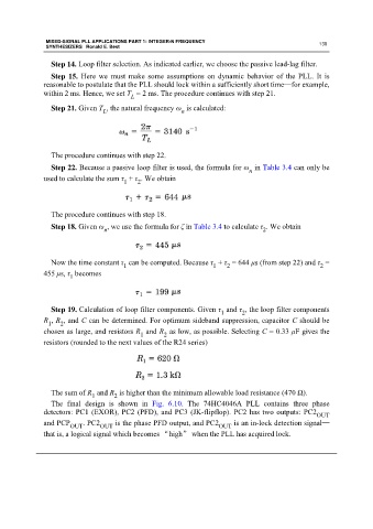
                 Step 21. Given T , the natural frequency ω  is calculated:
                                  L
                                                           n


                 The procedure continues with step 22.
                 Step 22. Because a passive loop filter is used, the formula for ω  in Table 3.4 can only be
                                                                                 n
               used to calculate the sum τ  + τ . We obtain
                                         1
                                             2


                 The procedure continues with step 18.

                 Step 18. Given ω , we use the formula for ζ in Table 3.4 to calculate τ . We obtain
                                  n                                                  2


                 Now the time constant τ  can be computed. Because τ  + τ  = 644 μs (from step 22) and τ =
                                        1                            1   2                             2
               455 μs, τ  becomes
                       1


                 Step 19. Calculation of loop filter components. Given τ  and τ , the loop filter components
                                                                       1      2
               R , R , and C can be determined. For optimum sideband suppression, capacitor C should be
                    2
                1
               chosen as large, and resistors R  and R  as low, as possible. Selecting C = 0.33 μF gives the
                                              1      2
               resistors (rounded to the next values of the R24 series)


                 The sum of R  and R  is higher than the minimum allowable load resistance (470 Ω).
                              1
                                     2
                 The final design is shown in  Fig. 6.10. The 74HC4046A PLL contains three phase
               detectors: PC1 (EXOR), PC2 (PFD), and PC3 (JK-flipflop). PC2 has two outputs: PC2
                                                                                                      OUT
               and PCP OUT  . PC2 OUT  is the phase PFD output, and PC2 OUT  is an in-lock detection signal—

               that is, a logical signal which becomes “high” when the PLL has acquired lock.

