
Page 210 - Power Electronic Control in Electrical Systems
P. 210
//SYS21/F:/PEC/REVISES_10-11-01/075065126-CH006.3D ± 198 ± [177±262/86] 17.11.2001 10:22AM
198 Power electronic equipment
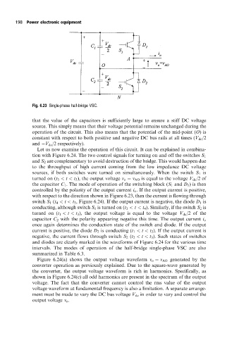
Fig. 6.23 Single-phase half-bridge VSC.
that the value of the capacitors is sufficiently large to ensure a stiff DC voltage
source. This simply means that their voltage potential remains unchanged during the
operation of the circuit. This also means that the potential of the mid-point (O)is
constant with respect to both positive and negative DC bus rails at all times (V dc /2
and V dc /2 respectively).
Let us now examine the operation of this circuit. It can be explained in combina-
tion with Figure 6.24. The two control signals for turning on and off the switches S 1
and S 2 are complementary to avoid destruction of the bridge. This would happen due
to the throughput of high current coming from the low impedance DC voltage
sources, if both switches were turned on simultaneously. When the switch S 1 is
turned on (t 3 < t < t 5 ), the output voltage v o v AO is equal to the voltage V dc /2 of
the capacitor C 1 . The mode of operation of the switching block (S 1 and D 1 ) is then
controlled by the polarity of the output current i o . If the output current is positive,
with respect to the direction shown in Figure 6.23, then the current is flowing through
switch S 1 (t 4 < t < t 5 , Figure 6.24). If the output current is negative, the diode D 1 is
conducting, although switch S 1 is turned on (t 3 < t < t 4 ). Similarly, if the switch S 2 is
turned on (t 1 < t < t 3 ), the output voltage is equal to the voltage V dc /2 of the
capacitor C 2 with the polarity appearing negative this time. The output current i o
once again determines the conduction state of the switch and diode. If the output
current is positive, the diode D 2 is conducting (t 1 < t < t 2 ). If the output current is
negative, the current flows through switch S 2 (t 2 < t < t 3 ). Such states of switches
and diodes are clearly marked in the waveforms of Figure 6.24 for the various time
intervals. The modes of operation of the half-bridge single-phase VSC are also
summarized in Table 6.3.
Figure 6.24(a) shows the output voltage waveform v o v AO generated by the
converter operation as previously explained. Due to the square-wave generated by
the converter, the output voltage waveform is rich in harmonics. Specifically, as
shown in Figure 6.24(c) all odd harmonics are present in the spectrum of the output
voltage. The fact that the converter cannot control the rms value of the output
voltage waveform at fundamental frequency is also a limitation. A separate arrange-
ment must be made to vary the DC bus voltage V dc in order to vary and control the
output voltage v o .