
Page 213 - Power Electronic Control in Electrical Systems
P. 213
//SYS21/F:/PEC/REVISES_10-11-01/075065126-CH006.3D ± 201 ± [177±262/86] 17.11.2001 10:22AM
Power electronic control in electrical systems 201
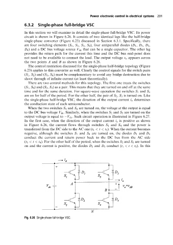
6.3.2 Single-phase full-bridge VSC
In this section we will examine in detail the single-phase full-bridge VSC. Its power
circuit is shown in Figure 6.26. It consists of two identical legs like the half-bridge
single-phase converter (Figure 6.23) discussed in Section 6.3.1. Specifically, there
are four switching elements (S 1 , S 2 , S 3 , S 4 ), four antiparallel diodes (D 1 , D 2 , D 3 ,
D 4 ) and a DC bus voltage source V dc that can be a single capacitor. The other leg
provides the return path for the current this time and the DC bus mid-point does
not need to be available to connect the load. The output voltage v o appears across
the two points A and B as shown in Figure 6.26.
The control restriction discussed for the single-phase half-bridge topology (Figure
6.23) applies to this converter as well. Clearly the control signals for the switch pairs
(S 1 , S 2 ) and (S 3 , S 4 ) must be complementary to avoid any bridge destruction due to
shoot through of infinite current (at least theoretically).
There are two control methods for this topology. The first one treats the switches
(S 1 , S 4 ) and (S 2 , S 3 ) as a pair. This means that they are turned on and off at the same
time and for the same duration. For square-wave operation the switches S 1 and S 4
are on for half of the period. For the other half, the pair of S 2 , S 3 is turned on. Like
the single-phase half-bridge VSC, the direction of the output current i o determines
the conduction state of each semiconductor.
When the two switches S 1 and S 4 are turned on, the voltage at the output is equal
to the DC bus voltage V dc . Similarly, when the switches S 2 and S 3 are turned on the
output voltage is equal to V dc . Such circuit operation is illustrated in Figure 6.27.
In the first case, when the direction of the output current i o is positive as shown
in Figure 6.26, the current flows through switches S 1 and S 4 and the power is
transferred from the DC side to the AC one (t 4 < t < t 5 ). When the current becomes
negative, although the switches S 1 and S 4 are turned on, the diodes D 1 and D 4
conduct the current and return power back to the DC bus from the AC side
(t 3 < t < t 4 ). For the other half of the period, when the switches S 2 and S 3 are turned
on and the current is positive, the diodes D 2 and D 3 conduct (t 1 < t < t 2 ). In this
Fig. 6.26 Single-phase full-bridge VSC.