
Page 216 - Power Electronic Control in Electrical Systems
P. 216
//SYS21/F:/PEC/REVISES_10-11-01/075065126-CH006.3D ± 204 ± [177±262/86] 17.11.2001 10:23AM
204 Power electronic equipment
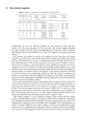
Table 6.4 Modes of operation of the single-phase full-bridge VSC
Switching device state Output Output Conducting Power
voltage current semiconductor transfer
S 1 S 2 S 3 S 4 v o v AB i o
Square-wave method or Phase-shifted method
1 0 0 1 V dc Positive S 1 S 4 t 4 < t < t 5 DC ! AC
1 0 0 1 V dc Negative D 1 D 4 t 3 < t < t 4 AC ! DC
0 1 1 0 V dc Negative S 2 S 3 t 2 < t < t 3 DC ! AC
0 1 1 0 V dc Positive D 2 D 3 t 1 < t < t 2 AC ! DC
Phase-shifted method only (extra modes ± free-wheeling modes)
1 0 1 0 0 Positive S 1 D 3 None
1 0 1 0 0 Negative S 3 D 1 None
0 1 0 1 0 Positive S 4 D 2 None
0 1 0 1 0 Negative S 2 D 4 None
synchronized in any way and the switches are not treated as pairs like pre-
viously. For the safe operation of the converter, the control signals between
(S 1 and S 2 ) and (S 3 and S 4 ) must be complementary. In this case, there is a phase-
shift between the two legs and this way a zero volts interval can appear across the
output.
For instance, if switches S 1 and S 3 are turned on at the same time, the output
voltage (v AB ) will be zero. The current in the case of other than unity power factor
must keep flowing. There is no power exchange between the DC side and the AC one
(free-wheeling mode). If the current is positive, the current flows through S 1 and D 3 .
If the current is negative, it flows through D 1 and S 3 . Similarly, when the two bottom
switches S 2 and S 4 are turned on at the same time, the output voltage (v AB ) is zero
and the output current once again determines which element conducts and allows the
output current to continue flowing. Specifically, if the current is positive, the diode
D 2 and the switch S 4 are conducting. In the case that the current is negative, the
switch S 2 and diode D 4 provide a path for the output current. These extra modes of
operation for the single-phase full-bridge topology (Figure 6.26) are also included in
Table 6.4 as the free-wheeling modes.
For a given phase-shift (a degrees) between the control signals of the two legs, the
waveforms are shown in Figure 6.29. It is clear that the output voltage waveform is a
three-level one, being able to have the values of V dc , 0 and V dc as shown in Figure
6.29(a). The control signals are shown in Figures 6.29(b)±(d). It is also clear that
between the top and bottom switches of each leg complementary control signals are
used. It should be noted that for a 0, the output voltage becomes similar to the
previously presented control method (square-wave, Figure 6.27(a)).
The output voltage v o (v AB ) is shown in Figure 6.30(a) along with the output
current i o and the DC bus current i d in Figures 6.30(b) and (c) respectively. Therefore,
by controlling the phase-shift between the two legs (a degrees), the rms value of the
fundamental component can be controlled. The amplitude of all odd harmonics, as
shown in Figure 6.30(d) for the output voltage, can also be controlled. The output
current has only a fundamental component as shown in Figure 6.30(e), where the DC
bus current has a DC component and all even harmonics as shown in Figure 6.30(f).