
Page 325 - Power Electronic Control in Electrical Systems
P. 325
//SYS21/F:/PEC/REVISES_10-11-01/075065126-CH008.3D ± 313 ± [290±372/83] 17.11.2001 10:28AM
Power electronic control in electrical systems 313
Ia Vcap Icap IIoad
212.0
Vs Vload 1.0
0.001
glbwd glfwd Iind 1.0
0.015 Vind
del Vs Source Voltage Vind Inductor Voltage
0.00666667
Zero Delay
Vs Detector zcross glfwd Vload Load Voltage Iind Inductor Current
Iload
Load Current Vcap Capacitor Voltage
Delay
A glbwd
0.0 Compar-
ator
zcross B Ia Source Current Icap Capacitor Current
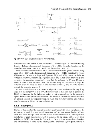
Fig. 8.27 TCSC basic circuit implemented in PSCAD/EMTDC.
constant and stable reference and it is taken as the input signal to the zero-crossing
detector. Taking a fundamental frequency of f 50 Hz, the delay function in the
controller is adjusted in order to obtain a firing angle of a 130 .
The waveforms of the simulated TCSC model are shown in Figure 8.28 for a firing
angle of a 130 and a fundamental frequency of f 50 Hz. Specifically, Figure
8.28(a) shows the source voltage and Figures 8.28(b) and 8.28(c) show the inductor
voltage and current, respectively. Figures 8.28(d) and 8.28(e) show the voltage and
current of the capacitor respectively. Note that the voltages V S , V L and V C are in
phase. It should also be noted that the zero-crossing of the source voltage V S
coincides with the negative peak of the inductor current I L and with the positive
peak of the capacitor current I C .
The characteristic waveforms shown in Figure 8.28 can be obtained for any firing
angle a in the range 90 < a < 180 . It is important to mention that in general the
TCSC performance in the inductive region is not as smooth as in the capacitive
region. In inductive operation conduction, the inductive current and the active losses
are greater than in the capacitive region. Also, the capacitor current and voltage
waveforms present higher harmonic distortion.
8.5.2 Example 2
The test system used in the example 2 is shown in Figure 8.29. Only one phase of the
test system is used. It comprises of a constant AC voltage source feeding a linear
series R±L load through three parallel branch transmission circuits. The equivalent
impedance of each transmission path is adjusted to be equal, with one of them
including a TCSC. As shown in Figure 8.29, the top branch contains a breaker,
Brk, which is used to simulate the opening of this branch at a given point in time of