
Page 271 - Power Electronics Handbook
P. 271
Chapter 12
D.C. to d.c. converters
12.1 Introduction
To regulate the power between a d.c. source and a d.c. load both linear
and switching techniques can be used. Linear regulators are simpler in
design and provide a smoother output with less RFI generation, but they
dissipate much more power within the regulator. Therefore for high-power
applications switching regulators are almost invariably used.
The basic switching d.c. to d.c. regulator was introduced in Chapter 6,
and it was shown there that both step-down and step-up controllers are
available. The step-down converter is the one most frequently used and
this is described in the next section, step-up converters being introduced in
Section 12.5.
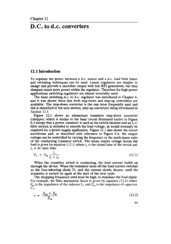
Figure 12.1 shows an elementary transistor stepdown converter
(chopper) which is similar to the basic circuit illustrated earlier in Figure
6.5 except that a power transistor is used as the switch element and an L-C
filter section is included to smooth the load voltage, as would normally be
required for a power supply application. Figure 12.1 also shows the circuit
waveforms and, as described with reference to Figure 6.6, the output
voltage can be controlled by varying the frequency or the mark-space ratio
of the conducting transistor switch. The mean output voltage across the
load is given by equation (12.1) where tc is the closed time of the switch and
to is its open time.
(12.1)
When the transistor switch is conducting, the load current builds up
through the device. When the transistor turns off the load current switches
to the free-wheeling diode D1 and the current slowly decays, until the
transistor is turned on again at the start of the next cycle.
The chopping frequency used must be high, to minimise the load ripple.
For example, the filter attenuation factor is given by equation (1 2.2) where
Zi, is the impedance of the inductor L, and Zc, is the impedance of capacitor
Cl.
2, + 2,
t= (12.2)
2,
26 I