
Page 51 - Power Quality in Electrical Systems
P. 51
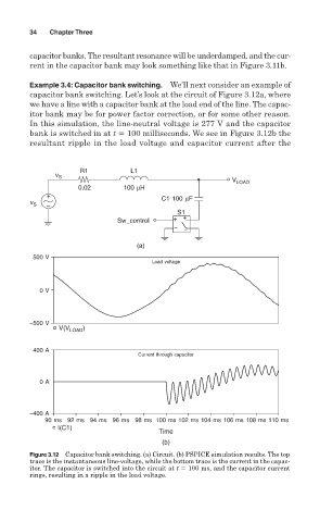
34   Chapter Three

        capacitor banks. The resultant resonance will be underdamped, and the cur-
        rent in the capacitor bank may look something like that in Figure 3.11b.

        Example 3.4: Capacitor bank switching. We’ll next consider an example of
        capacitor bank switching. Let’s look at the circuit of Figure 3.12a, where
        we have a line with a capacitor bank at the load end of the line. The capac-
        itor bank may be for power factor correction, or for some other reason.
        In this simulation, the line-neutral voltage is 277 V and the capacitor
        bank is switched in at t   100 milliseconds. We see in Figure 3.12b the
        resultant ripple in the load voltage and capacitor current after the


                     R1          L1
               v S
                                                           V LOAD
                    0.02        100 µH
             +                           C1 100 µF
         v S  −
                                             S1
                              Sw_control    +  +
                                            −  −

                                   (a)
         500 V
                                       Load voltage


           0 V


        −500 V
                V(V LOAD )

         400 A
                                   Current through capacitor


           0 A


        −400 A
            90 ms 92 ms 94 ms 96 ms 98 ms 100 ms 102 ms 104 ms 106 ms 108 ms 110 ms
               I(C1)
                                        Time
                                         (b)
        Figure 3.12 Capacitor bank switching. (a) Circuit. (b) PSPICE simulation results. The top
        trace is the instantaneous line-voltage, while the bottom trace is the current in the capac-
        itor. The capacitor is switched into the circuit at t   100 ms, and the capacitor current
        rings, resulting in a ripple in the load voltage.