
Page 53 - Power Quality in Electrical Systems
P. 53
36 Chapter Three
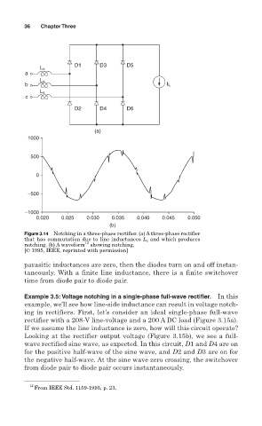
D1 D3 D5
L s
a
L s
b I L
L s
c
D2 D4 D6
(a)
1000
500
0
−500
−1000
0.020 0.025 0.030 0.035 0.040 0.045 0.050
(b)
Figure 3.14 Notching in a three-phase rectifier. (a) A three-phase rectifier
that has commutation due to line inductances L s and which produces
notching. (b) A waveform 12 showing notching.
[© 1995, IEEE, reprinted with permission]
parasitic inductances are zero, then the diodes turn on and off instan-
taneously. With a finite line inductance, there is a finite switchover
time from diode pair to diode pair.
Example 3.5: Voltage notching in a single-phase full-wave rectifier. In this
example, we’ll see how line-side inductance can result in voltage notch-
ing in rectifiers. First, let’s consider an ideal single-phase full-wave
rectifier with a 208-V line-voltage and a 200 A DC load (Figure 3.15a).
If we assume the line inductance is zero, how will this circuit operate?
Looking at the rectifier output voltage (Figure 3.15b), we see a full-
wave rectified sine wave, as expected. In this circuit, D1 and D4 are on
for the positive half-wave of the sine wave, and D2 and D3 are on for
the negative half-wave. At the sine wave zero crossing, the switchover
from diode pair to diode pair occurs instantaneously.
12
From IEEE Std. 1159-1995, p. 23.