
Page 46 - Power Quality in Electrical Systems
P. 46
Voltage Distortion 29
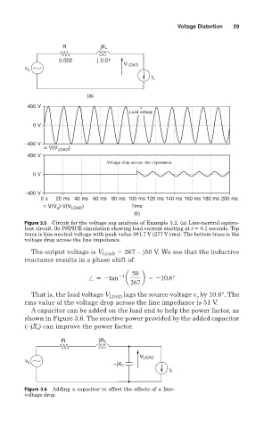
R jX L
0.002 j 0.01
V LOAD
v s
I L
(a)
400 V
Load voltage
0 V
−400 V
V(V LOAD )
400 V
Voltage drop across line impedance
0 V
−400 V
0 s 20 ms 40 ms 60 ms 80 ms 100 ms 120 ms 140 ms 160 ms 180 ms 200 ms
V(V )-V(V LOAD ) Time
s
(b)
Figure 3.5 Circuit for the voltage sag analysis of Example 3.2. (a) Line-neutral equiva-
lent circuit. (b) PSPICE simulation showing load current starting at t 0.1 seconds. Top
trace is line-neutral voltage with peak value 391.7 V (277 V rms). The bottom trace is the
voltage drop across the line impedance.
The output voltage is V LOAD 267 – j50 V. We see that the inductive
reactance results in a phase shift of:
50
tan 1 a b 10.6°
267
That is, the load voltage V LOAD lags the source voltage v by 10.6°. The
s
rms value of the voltage drop across the line impedance is 51 V.
A capacitor can be added on the load end to help the power factor, as
shown in Figure 3.6. The reactive power provided by the added capacitor
(–jX ) can improve the power factor.
c
R jX L
V LOAD
v s
−jX c
I L
Figure 3.6 Adding a capacitor to offset the effects of a line-
voltage drop.