
Page 125 - Rashid, Power Electronics Handbook
P. 125
112 S. Abedinpour and K. Shenai
in the base should be described by ambipolar transport cause different states of charge and therefore different capaci-
theory. tance values.
The stored charge in the lightly doped wide base of the
bipolar component of IGBT causes switching delays and
7.7.1 Input and Output Characteristics switching losses. The standard quasi-static charge description
is not adequate for IGBT because it assumes that the charge
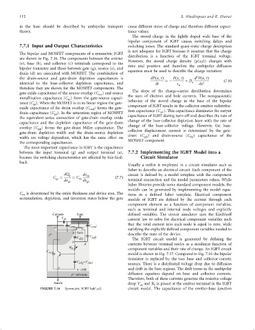
The bipolar and MOSFET components of a symmetric IGBT
distribution is a function of the IGBT terminal voltage.
are shown in Fig. 7.16. The components between the emitter
However, the stored charge density (p(x,t)) changes with
(e), base (b), and collector (c) terminals correspond to the time and position and therefore the ambipolar diffusion
bipolar transistor and those between gate (g), source (s), and
equation must be used to describe the charge variation:
drain (d) are associated with MOSFET. The combination of
2
the drain-source and gate-drain depletion capacitances is dPðx; tÞ Pðx; tÞ d Pðx; tÞ
¼ÿ þ D a ð7:8Þ
identical to the base-collector depletion capacitance, and dt t dx 2
a
therefore they are shown for the MOSFET components. The
The slope of the charge-carrier distribution determines
gate-oxide capacitance of the source overlap (C ) and source
oxs
metallization capacitance (C ) form the gate-source capaci- the sum of electron and hole currents. The nonquasistatic
m
tance (C ). When the MOSFET is in its linear region the gate- behavior of the stored charge in the base of the bipolar
gs
oxide capacitance of the drain overlap (C oxd ) forms the gate- component of IGBT results in the collector-emitter redistribu-
cer
drain capacitance (C ). In the saturation region of MOSFET tion capacitance (C ). This capacitance dominates the output
gd
the equivalent series connection of gate-drain overlap oxide capacitance of IGBT during turn-off and describes the rate of
change of the base-collector depletion layer with the rate of
capacitance and the depletion capacitance of the gate-drain
change of the base-collector voltage. However, the base-
overlap (C ) forms the gate-drain Miller capacitance. The
gdj
gate-drain depletion width and the drain-source depletion collector displacement current is determined by the gate-
drain (C ) and drain-source (C ) capacitance of the
gdj
dsj
width are voltage dependent, which has the same effect on MOSFET component.
the corresponding capacitances.
The most important capacitance in IGBT is the capacitance
between the input terminal (g) and output terminal (a), 7.7.2 Implementing the IGBT Model into a
because the switching characteristics are affected by this feed- Circuit Simulator
back.
Usually a netlist is employed in a circuit simulator such as
Saber to describe an electrical circuit. Each component of the
dQ g dv circuit is de®ned by a model template with the component
C ¼ ¼ C ox ox ð7:7Þ
ga
dv ga dv ga terminal connection and the model parameters values. While
Saber libraries provide some standard component models, the
models can be generated by implementing the model equa-
C is determined by the oxide thickness and device area. The
ox tions in a de®ned Saber template. Electrical component
accumulation, depletion, and inversion states below the gate models of IGBT are de®ned by the current through each
component element as a function of component variables,
such as terminal and internal node voltages and explicitly
de®ned variables. The circuit simulator uses the Kirchhoff
current law to solve for electrical component variables such
that the total current into each node is equal to zero, while
satisfying the explicitly de®ned component variables needed to
describe the state of the device.
The IGBT circuit model is generated by de®ning the
currents between terminal nodes as a nonlinear function of
component variables and their rate of change. An IGBT circuit
model is shown in Fig. 7.17. Compared to Fig. 7.16 the bipolar
transistor is replaced by the two base and collector-current
sources. There is a distributed voltage drop due to diffusion
and drift in the base regions. The drift terms in the ambipolar
diffusion equation depend on base and collector currents.
Therefore, both of these currents generate the resistive voltage
drop V and R is placed at the emitter terminal in the IGBT
ae
b
FIGURE 7.16 Symmetric IGBT half cell. circuit model. The capacitance of the emitter-base junction