
Page 122 - Rashid, Power Electronics Handbook
P. 122
7 Insulated Gate Bipolar Transistor 109
provide the required gate charge for zero current switching
and zero voltage switching. The delay of the input signal to the
gate drive should be small compared to the IGBT switching
period and therefore the gate drive speed should be designed
properly to be able to use the advantages of faster switching
speeds of the new generation IGBTs.
7.6.1 Conventional Gate Drives
The ®rst IGBT gate drives used ®xed passive components and
were similar to MOSFET gate drives. Conventional gate-drive
circuits use a ®xed gate resistance for turn-on and turn-off as
shown in Fig. 7.12.
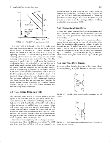
The turn-on gate resistor R gon limits the maximum collector
FIGURE 7.11 The IGBT safe operating area (SOA). current during turn-on, and the turn-off gate resistor R goff
limits the maximum collector-emitter voltage. In order to
The IGBT SOA is indicated in Fig. 7.11. Under short decouple the dv =dt and di =dt control an external capaci-
c
ce
switching times the rectangular SOA shrinks by an increase tance C can be used at the gate, which increases the time
g
in the duration of the on-time. Thermal limitation is the constant of the gate circuit and reduces the di =dt as shown in
c
reason for smaller SOA and the lower limit is set by dc Fig. 7.13. However, C does not affect the dv =dt transient,
ce
g
operating conditions. The device switching loci under hard which occurs during the Miller plateau region of the gate
switching (dashed lines) and zero voltage or zero current voltage.
switching (solid lines) is also indicated in Fig. 7.11. The
excursion is much wider for switch-mode hard-switching
applications than for the soft-switching case and therefore a 7.6.2 New Gate-Drive Circuits
much wider SOA is required for hard-switching applications.
In order to reduce the delay time required for the gate voltage
At present, IGBTs are optimized for hard-switching applica- ÿ
to increase from v to V ðthÞ, the external gate capacitor can
gg
ge
tions. In soft-switching applications the conduction losses of
IGBT can be optimized at the cost of smaller SOA. In this case
the p-base doping can be adjusted to result in a much lower
threshold voltage and hence forward voltage drop. However, in
hard-switching applications the SOA requirements dominate
over forward voltage drop and switching time. Therefore, the
p-base resistance should be reduced, which causes a higher
threshold voltage. As a result, the channel resistance and
forward voltage drop will increase.
7.6 Gate-Drive Requirements
FIGURE 7.12 Gate-drive circuit with independent turn-on and turn-off
The gate-drive circuit acts as an interface between the logic resistors.
signals of the controller and the gate signals of the IGBT,
which reproduces the commanded switching function at a
higher power level. Nonidealities of the IGBT such as ®nite
voltage and current rise and fall times, turn-on delay, voltage
and current overshoots, and parasitic components of the
circuit cause differences between the commanded and real
waveforms. Gate-drive characteristics affect the IGBT non-
idealities. The MOSFET portion of the IGBT drives the base of
the pnp-transistor and therefore the turn-on transient and
losses are greatly affected by the gate drive.
Due to lower switching losses, soft-switched power conver-
ters require gate drives with higher power ratings. The IGBT FIGURE 7.13 External gate capacitor for decoupling dv ce =dt and di c =dt
gate drive must have suf®cient peak current capability to during switching transient.