
Page 118 - Rashid, Power Electronics Handbook
P. 118
7 Insulated Gate Bipolar Transistor 105
fraction of the total voltage drop. When lifetime control
techniques are used to increase the switching speed, the
current gain of the bipolar transistor is reduced and a greater
portion of the current ¯ows through the MOSFET channel
and thus the voltage drop across the MOSFET increases. In
order to decrease the resistance of the MOSFET current path,
trench IGBTs can be used as is shown in Fig. 7.7. Extending the
ÿ
trench gate below the p-base and n -drift region junction
ÿ
þ
forms a channel between the n -emitter and the n -drift
region. This eliminates the JFET and accumulation layer
resistance and thus reduces the voltage drop across the
MOSFET component of IGBT, which results in superior
conduction characteristics. By use of trench structure the
IGBT cell density and latching current density are also
improved.
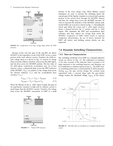
FIGURE 7.6 Components of on-state voltage drop within the IGBT
structure.
7.4 Dynamic Switching Characteristics
Because of the very low gain of the pnp-BJT, the driver
MOSFET in the equivalent circuit of the IGBT carries a major 7.4.1 Turn-on Characteristics
portion of the total collector current. Therefore, the IGBT on- The switching waveforms of an IGBT in a clamped inductive
state voltage drop as is shown in Fig. 7.6 consists of voltage circuit are shown in Fig. 7.8. The inductance-to-resistance
drop across the collector junction, drop across the drift region, (L=R) time constant of the inductive load is assumed to be
and the drop across the MOSFET portion. The low value of large compared to the switching frequency and therefore can
the drift-region conductivity modulation near the p-base be considered as a constant current source I . The IGBT turn-
on
junction causes a substantial drop across the JFET resistance on switching performance is dominated by its MOS structure.
of the MOSFET (V JFET ) in addition to the voltage drop across During t dðonÞ the gate current charges the constant input
the channel resistance (V ) and the accumulation layer capacitance with a constant slope until the gate-emitter
ch
resistance (V ): voltage reaches the threshold voltage V GEðthÞ of the device.
acc
V ¼ V þ þ V þ V ð7:2Þ
CEðonÞ p n drift MOSFET
V MOSFET ¼ V þ V JFET þ V acc ð7:3Þ
ch
ÿ
When the lifetime in the n -drift region is large, the gain of V GG +
the pnp-bipolar transistor is high and its collector current is V GE(Ion)
much larger than the MOSFET current. Therefore, the voltage v GE (t) V GE(th) t
drop across the MOSFET component of IGBT is a small
t d(on)
I on
i C (t) t
t ri
t fv2
V cc
V CE(on)
t fv1
v CE (t) t
FIGURE 7.8 The IGBT turn-on waveforms in a clamped inductive load
FIGURE 7.7 Trench IGBT structure. circuit.