
Page 120 - Rashid, Power Electronics Handbook
P. 120
7 Insulated Gate Bipolar Transistor 107
process in the portion of the drift region, which is not swept the injected holes into the drift region will be collected at the
ÿ
by the reverse bias. junction of p-base and n -drift regions. Therefore, the magni-
tude of the lateral hole current increases, which increases the
lateral voltage drop. As a result the parasitic thyristor will latch
7.4.3 Latch-up of Parasitic Thyristor up even if the on-state current is less than the static latch-up
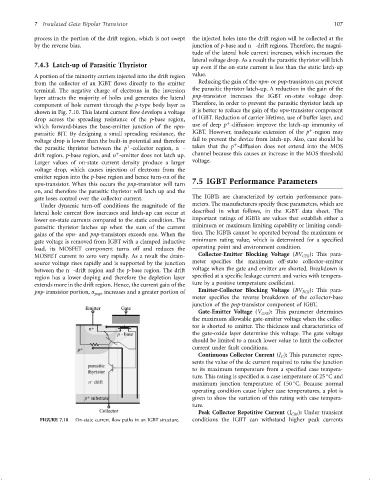
A portion of the minority carriers injected into the drift region value.
from the collector of an IGBT ¯ows directly to the emitter Reducing the gain of the npn-or pnp-transistors can prevent
terminal. The negative charge of electrons in the inversion the parasitic thyristor latch-up. A reduction in the gain of the
layer attracts the majority of holes and generates the lateral pnp-transistor increases the IGBT on-state voltage drop.
component of hole current through the p-type body layer as Therefore, in order to prevent the parasitic thyristor latch up
shown in Fig. 7.10. This lateral current ¯ow develops a voltage it is better to reduce the gain of the npn-transistor component
drop across the spreading resistance of the p-base region, of IGBT. Reduction of carrier lifetime, use of buffer layer, and
þ
which forward-biases the base-emitter junction of the npn- use of deep p -diffusion improve the latch-up immunity of
þ
parasitic BJT. By designing a small spreading resistance, the IGBT. However, inadequate extension of the p -region may
voltage drop is lower than the built-in potential and therefore fail to prevent the device from latch-up. Also, care should be
þ
ÿ
þ
the parasitic thyristor between the p -collector region, n - taken that the p -diffusion does not extend into the MOS
þ
drift region, p-base region, and n -emitter does not latch up. channel because this causes an increase in the MOS threshold
Larger values of on-state current density produce a larger voltage.
voltage drop, which causes injection of electrons from the
emitter region into the p-base region and hence turn-on of the
npn-transistor. When this occurs the pnp-transistor will turn 7.5 IGBT Performance Parameters
on, and therefore the parasitic thyristor will latch up and the
gate loses control over the collector current. The IGBTs are characterized by certain performance para-
Under dynamic turn-off conditions the magnitude of the meters. The manufacturers specify these parameters, which are
lateral hole current ¯ow increases and latch-up can occur at described in what follows, in the IGBT data sheet. The
lower on-state currents compared to the static condition. The important ratings of IGBTs are values that establish either a
parasitic thyristor latches up when the sum of the current minimum or maximum limiting capability or limiting condi-
gains of the npn- and pnp-transistors exceeds one. When the tion. The IGBTs cannot be operated beyond the maximum or
gate voltage is removed from IGBT with a clamped inductive minimum rating value, which is determined for a speci®ed
load, its MOSFET component turns off and reduces the operating point and environment condition.
MOSFET current to zero very rapidly. As a result the drain- Collector-Emitter Blocking Voltage (BV CES ): This para-
source voltage rises rapidly and is supported by the junction meter speci®es the maximum off-state collector-emitter
ÿ
between the n -drift region and the p-base region. The drift voltage when the gate and emitter are shorted. Breakdown is
region has a lower doping and therefore the depletion layer speci®ed at a speci®c leakage current and varies with tempera-
extends more in the drift region. Hence, the current gain of the ture by a positive temperature coef®cient.
pnp-transistor portion, a , increases and a greater portion of Emitter-Collector Blocking Voltage (BV ECS ): This para-
pnp
meter speci®es the reverse breakdown of the collector-base
junction of the pnp-transistor component of IGBT.
Gate-Emitter Voltage (V GES ): This parameter determines
the maximum allowable gate-emitter voltage when the collec-
tor is shorted to emitter. The thickness and characteristics of
the gate-oxide layer determine this voltage. The gate voltage
should be limited to a much lower value to limit the collector
current under fault conditions.
Continuous Collector Current (I ): This parameter repre-
C
sents the value of the dc current required to raise the junction
to its maximum temperature from a speci®ed case tempera-
ture. This rating is speci®ed at a case temperature of 25 C and
maximum junction temperature of 150 C. Because normal
operating condition cause higher case temperatures, a plot is
given to show the variation of this rating with case tempera-
ture.
Peak Collector Repetitive Current (I CM ): Under transient
FIGURE 7.10 On-state current ¯ow paths in an IGBT structure. conditions the IGBT can withstand higher peak currents