
Page 117 - Rashid, Power Electronics Handbook
P. 117
104 S. Abedinpour and K. Shenai
in NPTstructure the carrier lifetime is kept more than that of a
PT structure, which causes conductivity modulation of the
drift region and reduces the on-state voltage drop.
7.3 Static Characteristics
In the IGBT structure of Fig. 7.2 if a negative voltage is applied
þ
to the collector, the junction between the p -substrate and
ÿ
n -drift region becomes reverse-biased. The drift region is (a) (b)
lightly doped and the depletion layer extends principally into
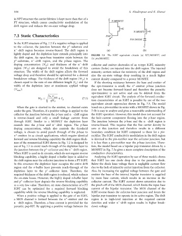
FIGURE 7.5 The IGBT equivalent circuits (a) BJT=MOSFET, and
the drift region. An open-base transistor exists between the (b) pin=MOSFET.
ÿ
þ
p -substrate, n -drift region, and the p-base region. The
ÿ
doping concentration (N ) and thickness of the n -drift collector and emitter electrodes of an n-type IGBT, minority
D
region (W ) are designed to avoid the breakdown of this carriers (holes) are injected into the drift region. The injected
D
structure. The width of the drift region affects the forward minority carriers reduce the resistivity of the drift region and
voltage drop and therefore should be optimized for a desired also the on-state voltage drop resulting in a much higher
breakdown voltage. The thickness of the drift region (W )is current density compared to a power MOSFET.
D
chosen equal to the sum of one diffusion length (L ) and the If the shorting resistance between the base and emitter of
p
width of the depletion layer at maximum applied voltage the npn-transistor is small, the n -emitter p-base junction
þ
(V max ): does not become forward-biased and therefore the parasitic
npn-transistor is not active and can be deleted from the
s
2e V max equivalent IGBT circuit. The analysis of the forward conduc-
s
W ¼ þ L p ð7:1Þ
D
qN tion characteristics of an IGBT is possible by use of the two
D
equivalent circuit approaches shown in Fig. 7.5. The model
When the gate is shorted to the emitter, no channel exists based on a pin-recti®er in series with a MOSFET shown in Fig.
under the gate. Therefore, if a positive voltage is applied to the 7-5b is easy to analyze and gives a reasonable understanding of
ÿ
collector the junction between the p-base and n -drift region the IGBToperation. However, this model does not account for
is reverse-biased and only a small leakage current ¯ows the hole-current component ¯owing into the p-base region.
ÿ
through IGBT. Similar to a MOSFET the depletion layer The junction between the p-base and the n -drift region is
ÿ
extends into the p-base and n -drift region. The p-base reverse-biased. This requires that the free carrier density be
doping concentration, which also controls the threshold zero at this junction and therefore results in a different
voltage, is chosen to avoid punch through of the p-base to boundary condition for IGBT compared to those for a pin-
þ
n -emitter. In ac circuit applications, which require identical recti®er. The IGBT conductivity modulation in the drift region
forward and reverse blocking capability the drift-region thick- is identical to the pin-recti®er near the collector junction, but
ness of the symmetrical IGBT shown in Fig. 7.2 is designed by it is less than a pin-recti®er near the p-base junction. There-
use of Eq. 7.1 to avoid reach-through of the depletion layer to fore, the model based on a bipolar pnp-transistor driven by a
ÿ
þ
the junction between the p -collector and the n -drift region. MOSFET in Fig. 7.5a gives a more complete description of the
When IGBT is used in dc circuits, which do not require reverse conduction characteristics.
blocking capability, a highly doped n-buffer layer is added to Analyzing the IGBT operation by use of these models shows
the drift region near the collector junction to form a PT IGBT. that IGBT has one diode drop due to the parasitic diode.
In this structure the depletion layer occupies the entire drift Below the diode knee voltage there is negligible current ¯ow
region and the n-buffer layer prevents reach-through of the due to the lack of minority carrier injection from the collector.
þ
depletion layer to the p -collector layer. Therefore, the Also, by increasing the applied voltage between the gate and
required thickness of the drift region is reduced, which reduces emitter the base of the internal bipolar transistor is supplied
the on-state losses. However, the highly doped n-buffer layer by more base current, which results in an increase in the
þ
and p -collector layer degrade the reverse blocking capability collector current. The IGBT current shows saturation due to
to a very low value. Therefore, on-state characteristics of a PT the pinch-off of the MOS channel, which limits the input base
IGBT can be optimized for a required forward blocking current of the bipolar transistor. The MOS channel of the
capability while the reverse blocking capability is neglected. IGBT reverse-biases the collector-base junction and forces the
When a positive voltage is applied to the gate of an IGBT, bipolar pnp-transistor to operate in its active region. The drift
þ
a MOS channel is formed between the n -emitter and the region is in high-level injection at the required current
ÿ
ÿ
n -drift region. Therefore, a base current is provided for the densities and wider n -drift region results in higher break-
parasitic pnp-BJT. By applying a positive voltage between the down voltage.