
Page 115 - Rashid, Power Electronics Handbook
P. 115
102 S. Abedinpour and K. Shenai
characteristics, good switching speed and excellent safe oper- of the model can follow only after the physics of device
ating area. Compared to power MOSFETs the absence of the operation under stress conditions imposed by the circuit is
integral body diode can be considered as an advantage or properly understood. Physically based process and device
disadvantage depending on the switching speed and current simulations are a quick and cheap way of optimizing the
requirements. An external fast-recovery diode or a diode in the IGBT. The emergence of mixed-mode circuit simulators in
same package can be used for speci®c applications. The IGBTs which semiconductor carrier dynamics is optimized within the
are replacing MOSFETs in high-voltage applications with constraints of circuit level switching is a key design tool for
lower conduction losses. They have on-state voltage and this task.
current density comparable to a power BJT with higher
switching frequency. Although they exhibit fast turn-on,
their turn-off is slower than a MOSFET because of current
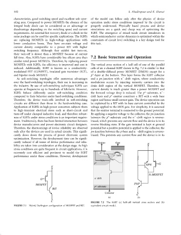
fall time. Also, IGBTs have considerably less silicon area than 7.2 Basic Structure and Operation
similar rated power MOSFETs. Therefore, by replacing power
MOSFETs with IGBTs, the ef®ciency is improved and cost is The vertical cross section of a half cell of one of the parallel
reduced. Additionally, IGBT is known as a conductivity- cells of an n-channel IGBT shown in Fig. 7.2 is similar to that
modulated FET (COMFET), insulated gate transistor (IGT), of a double-diffused power MOSFET (DMOS) except for a
þ
and bipolar-mode MOSFET. p -layer at the bottom. This layer forms the IGBT collector
ÿ
As soft-switching topologies offer numerous advantages and a pn-junction with n -drift region, where conductivity
over the hard-switching topologies, their use is increasing in modulation occurs by injecting minority carriers into the
the industry. By use of soft-switching techniques IGBTs can drain drift region of the vertical MOSFET. Therefore, the
operate at frequencies up to hundreds of kilohertz. However, current density is much greater than a power MOSFET and
ÿ
þ
IGBTs behave differently under soft-switching condition the forward voltage drop is reduced. The p -substrate, n -
þ
compared to their behavior under hard-switching conditions. drift layer and p -emitter constitute a BJT with a wide base
Therefore, the device trade-offs involved in soft-switching region and hence small current gain. The device operation can
circuits are different than those in the hard-switching case. be explained by a BJT with its base current controlled by the
Application of IGBTs in high-power converters subjects them voltage applied to the MOS gate. For simplicity, it is assumed
to high-transient electrical stress such as short-circuit and that the emitter terminal is connected to the ground potential.
turn-off under clamped inductive load, and therefore robust- By applying a negative voltage to the collector, the pn-junction
þ
ÿ
ness of IGBTs under stress conditions is an important require- between the p -substrate and the n -drift region is reverse-
ment. Traditionally, there has been limited interaction between biased, which prevents any current ¯ow and the device is in its
device manufacturers and power electronic circuit designers. reverse blocking state. If the gate terminal is kept at ground
Therefore, the shortcomings of device reliability are observed potential but a positive potential is applied to the collector, the
ÿ
only after the devices are used in actual circuits. This signi®- pn-junction between the p-base and n -drift region is reverse-
cantly slows down the process of power electronic system biased. This prevents any current ¯ow and the device is in its
optimization. However, the development time can be signi®-
cantly reduced if all issues of device performance and relia-
bility are taken into consideration at the design stage. As high
stress conditions are quite frequent in circuit applications, it is
extremely cost ef®cient and pertinent to model the IGBT
performance under these conditions. However, development
(a) (b)
FIGURE 7.2 The IGBT (a) half-cell vertical cross section and (b)
FIGURE 7.1 Hybrid Darlington con®guration of MOSFET and BJT. equivalent circuit model.