Page 110 - Rashid, Power Electronics Handbook
P. 110

96                                                                                            I. Batarseh

                                L               D                   where K oX  is the oxide relative dielectric constant, E denotes
                                                                                                               0
                                                        4           the   free-space  dielectric  constant  as  equal  to
                                                                    8:854   10 ÿ12  F=m; and T oX  is the oxide thickness layer as
                                       3                            given by data in Table 6.1.
                                                                      Finally, the diffusion and junction region capacitances
                                                                    between the bulk-to-channel (drain and source) are modeled
                                                                    by C BD  and C BS  across the two diodes. Because for almost all
                                            S                       power MOSFETS, the bulk and source terminals are connected
                                              1
                                                                    together and at zero potential, diodes D BD  and D BS  do not
                                                                    have forward bias, thereby resulting in very small conductance
                              5
                                                                    values, that is, small diffusion capacitances. The small signal
                                                                    model for MOSFET devices is given in Fig. 6.29.
                                           0
                                                                      EXAMPLE 6.4.  Figure 6.30a shows an example of a soft-
                                                                      switching power factor connection circuit that has two
                                                                      MOSFET. Its PSPICE simulation waveforms are shown
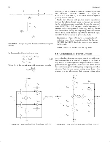
               FIGURE 6.27  Example of a power electronic circuit that uses a power
                                                                      in Fig. 6.30b.
               MOSFET.
                                                                      Table 6.2 shows the PSPICE code for Fig. 6.30a.

               In the saturation (linear) region we have            6.8 Comparison of Power Devices
                                     2
                               C GS  ¼ L C oX  þ C GSO
                                     3 W
                                                                    As stated earlier, the power electronic range is very wide, from
                               C GB  ¼ C GB0 L               ð6:48Þ
                                                                    hundreds of milliwatts to hundreds of megawatts and thus it is
                               C   ¼ C
                                GD    GD0                           very dif®cult to ®nd a single switching device type to cover all
               Where C oX  is the per-unit-area oxide capacitance given by  power electronic applications. Today's available power devices
                                                                    have tremendous power and frequency rating range, as well as
                                         K E
                                          oX 0
                                   C   ¼                            diversity. Their forward current ratings range from a few
                                     oX
                                          T
                                           oX                       amperes to a few kiloamperes, their blocking voltage rating
                                                                                           d
                                                                                          i
                                     Drain                                                 D
                                    i
                                     D                                                                   C
                                                                                            R D           BD
                                               C
                                      r         BD
                                      D
                                                                                C gd       d'            g BD
                             C
                              gd            i
                                             BD
                          +  V   -    +      -    +
                              GD               V
                                                BD
                                                                                             g V '
                                                                                              m  gs  g
                 Gate                                    Bulk(Substrate)                    +g V '    o            i
                               i      V                                i                      mb  bs               b
                               DS      DS              i               G
                      i                                B                                              -  V '  +
                      G                                                                                   BS
                                      -      -  V BS +                           C gs
                             C
                              gs
                                            i
                                            BS
                                                                             +   V '  -    S'            g
                          +      -                                                GS                      BS
                             V
                              GS
                                               C                                            R
                                      r         BS                                           S           C
                                      S                                                                   BS
                             C                                                  C
                              gb                                                  gb
                                    i                                                     i S
                                     S
                  FIGURE 6.28  Large-signal model for the n-channel MOSFET.  FIGURE 6.29  Small signal equivalent circuit model for MOSFET.
   105   106   107   108   109   110   111   112   113   114   115