
Page 109 - Rashid, Power Electronics Handbook
P. 109
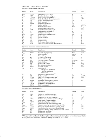
TABLE 6.1  PSPICE MOSFET parameters
                                (a) Device dc and parasitic parameters

                                Symbol   Name      Description                            Default   Units
                                Level    LEVEL     Model type (1, 2, 3, or 4)             1
                                         VTO       Zero-bias threshold voltage            0         V
                                V TO
                                l        LAMDA     Channel-length modulation 1,2a         0         v-1
                                g        GAMMA     Body-effect (bulk) threshold parameter  0        v ÿ1=2
                                F r      PHI       Surface inversion potential            0.6       V
                                Z        ETA       Static feedback 3                      0
                                k        KAPPA     Saturation ®eld factor 3               0.2
                                                                                                      2
                                         UO        Surface mobility                       600       cm =V-s
                                m 0
                                Is       IS        Bulk saturation current                10 ÿ14    A
                                Js       JS        Bulk saturation current=area           0         A=m 2
                                         JSSW      Bulk saturation current=length         0         A=m
                                J SSW
                                N        N         Bulk emission coef®cient n             1
                                         PB        Bulk junction voltage                  0.8       V
                                P B
                                         PBSW      Bulk sidewall diffusion voltage        PB        V
                                P BSW
                                R D      RD        Drain resistance                       0         O
                                R S      RS        Source resistance                      0         O
                                R G      RG        Gate resistance                        0         O
                                R B      RB        Bulk resistance                        0         O
                                         RDS       Drain-source shunt resistance          a         O
                                R ds
                                         RSH       Drain and source diffusion sheet resistance  0   O=m 2
                                R sh
                                (b) Device process and dimensional parameters
                                Symbol   Name      Description                            Default   Units
                                         NSUB      Substrate doping density               None      cm ÿ3
                                N sub
                                W        W         Channel width                          DEFW      m
                                L        L         Channel length                         DEFL      m
                                         WD        Lateral diffusion width                0         m
                                W D
                                X jl     LD        Lateral diffusion length               0         m
                                Kp       KP        Transconductance coef®cient            20   10 ÿ6  A=v 2
                                t 0X     TOX       Oxide thickness                        10 ÿ7     m
                                N SS     NSS       Surface-state density                  None      cm ÿ2
                                         NFS       Fast surface-state density             0         cm ÿ2
                                N FS
                                         NSUB      Substrate doping                       0         cm ÿ3
                                N A
                                         TPG       Gate material                          1
                                T PG
                                                      þ1 Opposite of substrate
                                                      ÿ1 Same as substrate
                                                      0 Aluminum
                                         XJ        Metallurgical junction depth 2,3       0         m
                                X j
                                                                                                      2
                                         UO        Surface mobility                       600       cm =V-s
                                m 0
                                         UCRIT     Mobility degradation critical ®eld 2   10 4      V=cm
                                U c
                                         UEXP      Mobility degradation exponent 2        0
                                U e
                                         VMAX      Maximum drift velocity of carriers 2   0         m=s
                                U t
                                         NEFF      Channel charge coef®cient 2            1
                                N eff
                                d        DELTA     Width effect on threshold 2,3          0
                                y        THETA     Mobility modulation 3                  0
                                (c) Device capacitance parameters
                                Symbol   Name      Description                            Default   Units
                                         CBD       Bulk-drain zero-bias capacitance       0         F
                                C BD
                                         CBS       Bulk-source zero-bias capacitance      0         F
                                C BS
                                         CJ        Bulk zero-bias bottom capacitance      0         F=m 2
                                C j
                                         CJSW      Bulk zero-bias perimeter capacitance=length  0   F=m
                                C jsw
                                         MJ        Bulk bottom grading coef®cient         0.5
                                M j
                                         MJSW      Bulk sidewall grading coef®cient       0.33
                                M jsw
                                         FC        Bulk forward-bias capacitance coef®cient  0.5
                                F C
                                         CGSO      Gate-source overlap capacitance=channel width  0  F=m
                                C GSO
                                XCGDO    CGDO      Gate-drain overlap capacitance=channel width  0  F=m
                                         CGBO      Gate-bulk overlap capacitance=channel length  0  F=m
                                C GBO
                                         XQC       Fraction of channel charge that associates with drain 1,2  0
                                X QC
                                         KF        Flicker noise coef®cient               0
                                K F
                                         AF        Flicker noise exponent                 0
                                a F
                                a
                                 All superscript numbers in the Description column indicate that this=these parameter(s) are available
                                in this=these level number(s), otherwise it=they are available in all levels.