Page 104 - Rashid, Power Electronics Handbook
P. 104

90                                                                                            I. Batarseh

               Notice that the MOSFET sustains high voltage and current
               simultaneously during intervals Dt 21  and Dt . This results in
                                                   32
               large power dissipation during turn-on, which contributes to
               overall switching losses. The smaller the R , the smaller Dt 21
                                                  G
               and Dt 32  become.
               6.6.3 Turn-off Characteristics

               To study the turn-off characteristic of the MOSFET, we will
               consider Fig. 6.17b again by assuming the MOSFET is on and
               in steady state at t > t with the equivalent circuit of Fig.
                                   0
               6.18(e). Therefore, at t ¼ t we have the following initial
                                       0
               conditions:
                               v ðt Þ¼ I r
                               DS 0
                                       D DSðONÞ
                               v ðt Þ¼ V GG
                               GS 0
                               t ðt Þ¼ I 0
                               DS 0
                                                             ð6:29Þ
                                i ðt Þ¼ 0
                                  0
                                G
                              v ðt Þ¼ V GG
                                  0
                               c GS
                              v  ðt Þ¼ V  ÿ I r
                               C GD  0  GG   0 DSðONÞ
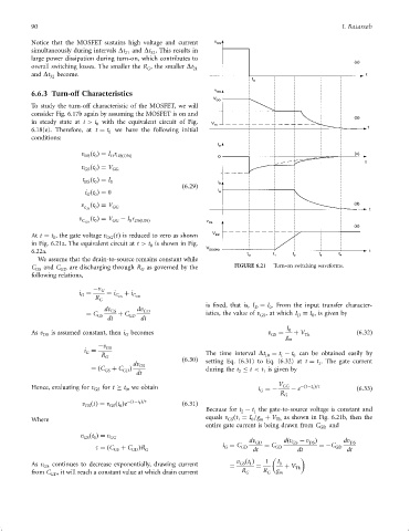
               At t ¼ t , the gate voltage v GG ðtÞ is reduced to zero as shown
                      0
               in Fig. 6.21a. The equivalent circuit at t > t is shown in Fig.
                                                   0
               6.22a.
                 We assume that the drain-to-source remains constant while
               C GS  and C GD  are discharging through R as governed by the  FIGURE 6.21  Turn-on switching waveforms.
                                                G
               following relations,
                                  ÿn
                              i ¼   G  ¼ i  þ i
                              G          C GS  C GD
                                   R G
                                                                    is ®xed, that is, I ¼ I . From the input transfer character-
                                     dv GS     dv GD                               D   0
                                ¼ C       þ C                       istics, the value of v , at which I ¼ I , is given by
                                   GS        GD                                     GS          D   0
                                      dt        dt
                                                                                            I 0
               As v DS  is assumed constant, then i becomes                            v GS  ¼  þ V Th            ð6:32Þ
                                            G
                                                                                            g m
                                    ÿv GS
                               i ¼
                                G
                                     R                              The time interval Dt 10  ¼ t ÿ t can be obtained easily by
                                                                                              0
                                                                                           1
                                      G                      ð6:30Þ
                                              dv GS                 setting Eq. (6.31) to Eq. (6.32) at t ¼ t . The gate current
                                                                                                      1
                                 ¼ðC  GS  þ C GD Þ                  during the t   t < t is given by
                                               dt                             2      1
                                                                                          V
               Hence, evaluating for v GS  for t   t , we obtain                    i ¼ÿ   GG  ÿ e ÿðtÿt 0 Þ=t    ð6:33Þ
                                            0
                                                                                    G
                                                                                          R G
                                            ÿðtÿt 0 Þ=t
                               v ðtÞ¼ v ðt Þe                ð6:31Þ
                                GS
                                       GS 0
                                                                    Because for t ÿ t the gate-to-source voltage is constant and
                                                                               2
                                                                                  1
                                                                    equals v ðt ¼ I =g þ V  as shown in Fig. 6.21b, then the
               Where                                                       GS 1   0  m   Th
                                                                    entire gate current is being drawn from C GD  and
                              v ðt Þ¼ v GG
                               GS 0
                                                                                 dv GD     dðv GS  ÿ v Þ     dv DS
                                                                                                   DS
                                   t ¼ðC GS  þ C GD ÞR G                 i ¼ C GD  dt  ¼ C GD   dt    ¼ÿC  GD  dt
                                                                          G

               As v GS  continues to decrease exponentially, drawing current  ¼  v ðt Þ  ¼  1  I 0  þ V Th
                                                                              GS 1
               from C  , it will reach a constant value at which drain current  R G  R G  g m
                     GD
   99   100   101   102   103   104   105   106   107   108   109