Page 100 - Rashid, Power Electronics Handbook
P. 100

86                                                                                            I. Batarseh

                 Capacitance                                                                             +V DD
                                           C
                                            gs


                                                                                                   L
                                                                                                    O            D
                                                       C
                                                        gd
                                                                                                        i
                                                                                                         D
                                                                                            C
                                                                                             GD
                                                        Voltage


                                                                                   R
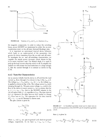
                   FIGURE 6.16  Variation of C gd and C gs as a function of v DS .   G
                                                                                        i
               the magnetic components. In order to reduce the switching                 G
               losses, power MOSFET are maintained in either the on-state  +
                                                                    v GG  -                   C GS
               (conduction state) or the off-state (forward-blocking) state.
                 It is important we understand internal device behavior,
               which leads to an understanind of the parameters that
               govern the device transition from the on-state and off-states.            (a)
               To investigate the on- and off-switching characteristics, we
                                                                                                          +V
               consider the simple power electronic circuit shown in Fig.                                   DD
               6.17a under inductive load. The ¯yback diode D is used to
               pick up the load current when the switch is off. To simplify the
               analysis we will assume the load inductance is a large enough
                                                                                                    I
               L that the current through it is constant as shown in Fig.                           O             D
                0
               6.17b.
                                                                                                          i
               6.6.2 Turn-On Characteristics
                                                                                                          D
               Let us assume initially that the device is off and that the load              C
                                                                                              G
               current I , ¯ows through D as shown in Fig. 6.18a, v GG  ¼ 0.                  D
                       0
               The voltage v DS  ¼ V DD  and i ¼ i .At t ¼ t , the voltage v GG
                                       G
                                           D
                                                    0
               is applied as shown in Fig. 6.19a. The voltage across C GS  starts
               charging through R . The gate-source voltage, v GS  controls the
                               G
               ¯ow of the drain-to-source current i . Let us assume that for        R G
                                             D
               t   t < t , v GS  < V , that is, the MOSFET remains in the                 i
                0
                       1
                                Th
               cut-off region with i ¼ 0, regardless of v . The time interval             G
                                D
                                                 DS
               ðt 1; t Þ represents the delay turn-on time needed to change  v  +               C G
                    0
                 2
               C GS  from zero to V . The expression for the time interval  GG  -               S
                                Th
               Dt ¼ t ÿ t can be obtained as shown next.
                 10   1   0
                 The gate current is given by
                                                                                          (b)
                                v GG  ÿ v GS
                           i ¼                                      FIGURE 6.17  (a) Simpli®ed equivalent circuit used to study turn-on
                            G
                                  R G                               and turn-off characteristics of the MOSFET; and (b) simpli®ed equivalent
                              ¼ i  þ i                       ð6:13Þ  circuit.
                                c GS  c GD
                                   dv GS     dðv ÿ v Þ
                                                    D
                                                G
                              ¼ C      ÿ C
                                 GS       GD                        then i is given by
                                    dt          dt                       G
               where v G  and v D  are gate-to-ground and drain-to-ground  i ¼ C  dv GS  þ C  dv GS  ¼ðC  þ C  Þ  dv GS  ð6:14Þ
               voltages, respectively. As we have v ¼ v , v ¼þV  ,      G    GS  dt    GD  dt     GS   GD  dt
                                               G    GS  D      DD
   95   96   97   98   99   100   101   102   103   104   105