
Page 95 - Rashid, Power Electronics Handbook
P. 95
6 The Power MOSFET 81
Drain (D)
Drain(D)
D
i
D
-
+
+
v
V V Gate (G) DS
GD DS
+ (G)
- _
+
Gate(G) v
GS -
+ Source(S) (S)
V -
GS
Source (S)
(a)
(a) (b)
i D Triode Saturation region (active
D D (linear region) region)
v <v -V v > v -V
DS GS Th DS GS Th
G G V increases
GS
V =V +1
GS Th
S S
(c) (d) V GS <V Th
v
DS
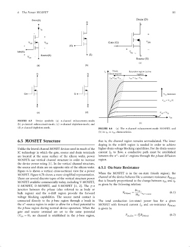
FIGURE 6.5 Device symbols: (a) n-channel enhancement-mode;
(b)
(b) p-channel enhancement-mode; (c) n-channel depletion-mode; and
(d) p-channel depletion-mode. FIGURE 6.6 (a) The n-channel enhancement-mode MOSFET; and
(b) its i D vs v DS characteristics.
6.5 MOSFET Structure that is, the channel region remains unmodulated. The lower
doping in the n-drift region is needed in order to achieve
Unlike the lateral channel MOSET devices used in much of the higher drain voltage blocking capabilities. For the drain-source
IC technology in which the gate, source and drain terminals current I D to ¯ow, a conductive path must be established
ÿ
þ
are located at the same surface of the silicon wafer, power between the n - and n -regions through the p-base diffusion
MOSFETs use vertical channel structure in order to increase region.
the device power rating [1]. In the vertical channel structure,
the source and drain are on opposite side of the silicon wafer. 6.5.1 On-State Resistance
Figure 6.7a shows a vertical cross-sectional view for a power
MOSFET. Figure 6.7b shows a more simpli®ed representation. When the MOSFET is in the on-state (triode region), the
channel of the device behaves like a constant resistance R
There are several discrete types of the vertical structure power DSðonÞ
MOSFET available commercially today, including V-MOSFET, that is linearly proportional to the change between v DS and i D
U-MOSFET, D-MOSFET, and S-MOSFET [1, 2]. The p-n as given by the following relation:
junction between the p-base (also referred to as body or @n DS
bulk region) and the n-drift region provide the forward R DSðonÞ ¼ j v GS¼Constant ð6:1Þ
@i D
voltage blocking capabilities. The source metal contact is
connected directly to the p-base region through a break in The total conduction (on-state) power loss for a given
þ
the n -source region in order to allow for a ®xed potential to MOSFET with forward current I D and on-resistance R DSðonÞ
the p-base region during normal device operation. When the is given by
gate and source terminal are set to the same potential 2
(V GS ¼ 0), no channel is established in the p-base region, P on;diss ¼ I R ð6:2Þ
D DSðonÞ