Page 93 - Rashid, Power Electronics Handbook
P. 93

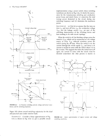
6 The Power MOSFET                                                                                   79

                                      i                                 implementation using a power switch whose switching
                                       sw
                                            +                           waveforms are shown in Fig. 6.4a; (b) derive the expres-
                                                                        sions for the instantaneous switching and conduction
                                           v
                                            sw                          power losses and sketch them; (c) determine the total
                                                                        average power dissipated in the circuit during one
                                            _
                                                                        switching frequency; and (d) determine the maximum
                    v                                                   power.
                     sw
                                                                        SOLUTION 6.2.  (a) First let us assume that the turn-on
                                    Forward voltage drop                time t  and turn-off time t , the conduction voltage
                  V                                                          on                 off
                   off                                                  V   , and the leakage current I  , are part of the
                                                                          ON                        OFF
                                                                        switching characteristics of the switching device and
                  V                                           time
                   on                                                   have nothing to do with circuit topology.
                    i                Turn-ON           Turn-OFF           When the switch is off, the blocking voltage across the
                     sw              switching         switching        switch is V OFF , which can be represented as a dc voltage
                                      delays            delays
                  I                                                     source of value V OFF  re¯ected somehow across the
                  on
                                                                        switch during the off-state. When the switch is on, the
                                                                        current through the switch equals I ON , and hence a dc
                                                                        current is needed in series with the switch when it is in
                  I                                           time
                   off
                                                                        the on-state. This suggests that when the switch turns off
                                                                        again, the current in series with the switch must be
                                    Leakage current
                                                                        diverted somewhere else (this process is known as
                    p(t)
                                      switching
                                       losses
                                                                                          v sw  i sw
                 P                                                             V  of
                  max
                                                                      i         f
                                                                       sw      I
                                                                                on
                                                              time         +
                                                                                                                I off
                                                                          v    V on                                   t
                                                                           sw
                                   conduction losses                                 t=0  t              t
                                                                           _              on             off
                                        T                                                      T
                                         s                                                      s
                                        (a)                                                      (a)
                                   Typical practical
                           i         waveform
                            sw                  (Highly Inductive load)         i
                                                                                 sw
                                          ON   OFF                                 +  v  -
                         ON                                                          sw                   S
                                                                                V off      R        V off        Load
                                        OFF
                                                          ON
                         ON         ON
                                        OFF
                   (Ideal Switch)                         OFF                                  (b)
                         OFF
                                       ON
                                        (Resistive                               P sw ()t
                                         load)
                                                                v
                                                                sw
                                   ON   OFF                                  I V
                                          (b)                                 on  off
                                                                               4
                 FIGURE 6.3  (a) Practical switching current, voltage and power wave-
                 forms; and (b) switching trajectory.                                                                t
                                                                                       0   t      T - t    T
                                                                                        t   on     s  off  t  s
                                                                                        on              off
                 Figure 3(b) shows several switching trajectories for the ideal          2      (c)     2
                 and practical cases under resistive loads.
                    EXAMPLE 6.2.  Consider a linear approximation of Fig.  FIGURE 6.4  Linear approximation of typical current and voltage
                    6.3a as shown in Fig. 6.4a: (a) give a possible circuit  switching waveforms.
   88   89   90   91   92   93   94   95   96   97   98