Page 94 - Rashid, Power Electronics Handbook
P. 94
80 I. Batarseh
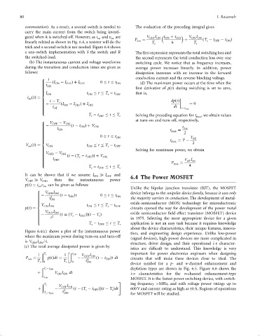
commutation). As a result, a second switch is needed to The evaluation of the preceding integral gives
carry the main current from the switch being investi-
I
I
gated when it is switched off. However, as i sw and v sw are P ¼ V OFF ON t ON þ t OFF þ V ON ON ðT ÿ t ÿ t Þ
linearly related as shown in Fig. 6.4, a resistor will do the ave T 6 T s OFF ON
s s
trick and a second switch is not needed. Figure 6.4 shows
a one-switch implementation with S the switch and R The ®rst expression represents the total switching loss and
the switched-load. the second represents the total conduction loss over one
(b) The instantaneous current and voltage waveforms switching cycle. We notice that as frequency increases,
during the transition and conduction times are given as average power increases linearly. In addition, power
follows: dissipation increases with an increase in the forward
t
8 conduction current and the reverse-blocking voltage.
> ðI ON ÿ I OFF Þþ I OFF 0 t t ON (d) The maximum power occurs at the time when the
>
> t
> ON
>
> ®rst derivative of pðtÞ during switching is set to zero,
>
>
>
< I ON t ON t T ÿ t OFF that is,
s
i ðtÞ¼
sw
> t ÿ T dpðtÞ
> s
> ÿ ðI ÿ I Þþ I ¼ 0
> ON OFF OFF
>
> t dt
> off t¼t max
>
>
:
T ÿ t OFF t T s Solving the preceding equation for t max , we obtain values
s
at turn-on and turn-off, respectively,
8
V OFF ÿ V ON
> ÿ ðt ÿ t Þþ V
> ON ON
> t
> t rise
> ON t ¼
> max
> 2
>
>
> 0 t t
> ON T
> fall
> t ¼ T ÿ
< max
V ðtÞ¼ V ON t ON t T ÿ t OFF 2
sw
s
>
> Solving for maximum power, we obtain
>
>
> V OFF ÿ V ON
>
> ðt ÿðT ÿ t ÞÞ þ V
> s OFF ON
> t
> OFF V I
> off on
>
> P max ¼
: 4
T ÿ t OFF t T s
s
It can be shown that if we assume I ON I OFF and 6.4 The Power MOSFET
V OFF V ON , then the instantaneous power
pðtÞ¼ i v can be given as follows:
sw sw
Unlike the bipolar junction transistor (BJT), the MOSFET
8
V I device belongs to the unipolar device family, because it uses only
> OFF ON
> ÿ ðt ÿ t Þt 0 t t
> 2 ON ON
> t the majority carriers in conduction. The development of metal-
> ON
>
>
> oxide-semiconductor (MOS) technology for microelectronic
< V I t t T ÿ t
pðtÞ¼ ON ON ON s OFF circuits opened the way for development of the power metal
> V I
> OFF ON oxide semiconductor ®eld effect transistor (MOSFET) device
> ÿ ðt ¼ðT ÿ t ÞÞðt ÿ T Þ
> s OFF s
> 2
> t in 1975. Selecting the most appropriate device for a given
>
>
:
T ÿ t OFF t T s application is not an easy task because it requires knowledge
s
about the device characteristics, their unique features, innova-
Figure 6.4(c) shows a plot of the instantaneous power
tion, and engineering design experience. Unlike low-power
where the maximum power during turn-on and turn-off
(signal devices), high-power devices are more complicated in
I
is V OFF ON =4. structure, driver design, and their operational i-v character-
(c) The total average dissipated power is given by
istics are dif®cult to understand. This knowledge is very
ð ð important for power electronics engineers when designing
1 T s 1 t ON V OFF ON
I
P ave ¼ pðtÞdt ¼ ÿ 2 ðt ÿ t ON Þtdt circuits that will make these devices close to ideal. The
T s 0 T s 0 t ON
device symbol for a p- and n-channel enhancement and
ð
T s ÿt OFF depletion types are shown in Fig. 6.5. Figure 6.6 shows the
I
þ V ON ON dt i-v characteristics for the n-channel enhancement-type
t ON
MOSFET. It is the fastest power switching device, with switch-
#
ð ing frequency >MHz, and with voltage power ratings up to
T s V I
þ ÿ OFF ON ðt ÿðT ÿ t OFF ÞÞðt ÿ T Þdt 600 V and current rating as high as 40 A. Regions of operations
s
s
t 2
T s ÿt OFF OFF for MOSFET will be studied.

