
Page 98 - Rashid, Power Electronics Handbook
P. 98
84 I. Batarseh
For a triode mode of operation, we have
i D
v GD > V Th
v GD < V Th
And for the saturation region of operation, pinch-off occurs
when v ¼ V .
GD Th
In terms v , the preceding inequalities may be expressed as
DS
follows.
1. For triode region of operation V Th v GS
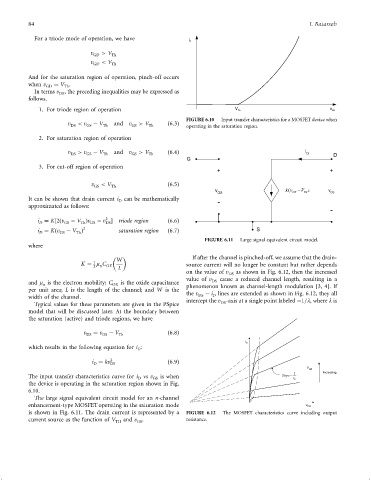
FIGURE 6.10 Input transfer characteristics for a MOSFET device when
v < v ÿ V and v > V ð6:3Þ
DS GS Th GS Th operating in the saturation region.
2. For saturation region of operation
v DS > v GS ÿ V Th and v GS > V Th ð6:4Þ i D D
G
3. For cut-off region of operation
+ +
v < V ð6:5Þ
GS Th
v k (v GS - V Th ,2 v
GS DS
It can be shown that drain current i can be mathematically -
D
approximated as follows:
-
2
i ¼ K2ðv GS ÿ V Þv DS ÿ v triode region ð6:6Þ
DS
Th
D
i ¼ Kðv ÿ V Þ 2 saturation region ð6:7Þ S
D GS Th
FIGURE 6.11 Large signal equivalent circuit model.
where
If after the channel is pinched-off, we assume that the drain-
W
1
K ¼ m C source current will no longer be constant but rather depends
2 n OX
L
on the value of v DS as shown in Fig. 6.12, then the increased
value of v DS cause a reduced channel length, resulting in a
and m is the electron mobility; C OX is the oxide capacitance phenomenon known as channel-length modulation [3, 4]. If
n
per unit area; L is the length of the channel; and W is the
the v DS ÿ i lines are extended as shown in Fig. 6.12, they all
D
width of the channel.
intercept the v -axis at a single point labeled ÿ1=l, where l is
DS
Typical values for these parameters are given in the PSpice
model that will be discussed later. At the boundary between
the saturation (active) and triode regions, we have
v DS ¼ v GS ÿ V Th ð6:8Þ
i D
which results in the following equation for i :
D
i ¼ kv 2 DS ð6:9Þ
D
v
GS
1 Increasing
The input transfer characteristics curve for i vs v GS is when Slope = O r
D
the device is operating in the saturation region shown in Fig.
6.10.
The large signal equivalent circuit model for an n-channel
enhancement-type MOSFET operating in the saturation mode v DS
is shown in Fig. 6.11. The drain current is represented by a FIGURE 6.12 The MOSFET characteristics curve including output
current source as the function of V TH and v . resistance.
GS