Page 102 - Rashid, Power Electronics Handbook
P. 102

88                                                                                            I. Batarseh

               From Eqs. (13) and (14), we obtain,                      v
                                                                         GG
                             V GG  ÿ v GS          dv GS                V                                     (a)
                           ;          ¼ðC GS  þ C GD Þ       ð6:15Þ      GG
                                R G                 dt

               Solving Eq. (6.15) for v ðtÞ for t > t with v ðt Þ¼ 0, we    t o
                                                      GS 0
                                               0
                                   GS
               obtain,
                                                                        v
                                                                         GG
                              v ðtÞ¼ V   ð1 ÿ e ðtÿt 0 Þ=t Þ  ð6:16Þ    v
                               GS      GG                                GS
               where
                                                                                                              (b)
                                 t ¼ R ðC  þ C  Þ                       V
                                     G  GS    GD                         Th
               The gate current i is given by
                              G
                                     v GG  ÿ v GS                           t o      t 1         t 2     t 3       t
                                 i ¼
                                  G
                                        R G
                                     V GG ÿðtÿt 0 Þ=t        ð6:17Þ      i G
                                 i ¼     e
                                  G
                                      R G
               As long as v GS  < V , i remains zero. At t ÿ t , v GS  reaches                                (c)
                                   D
                                                       1
                               Th
               V , causing the MOSFET to start conducting. Waveforms for
                 Th
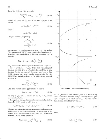
               i and v GS  are shown in Fig. 6.19. The time interval ðt ÿ t Þ is
                                                           1
                G
                                                              0
               given by                                              - V GG - VTh
                                                                       R G

                                                  V Th                   i D
                           Dt  ¼ t ÿ t ¼ÿt ln 1 ÿ
                             10  1   0
                                                  V GG                   I
                                                                          O
               Dt 10  represents the ®rst delay interval in the turn-on process.
                 For t > t with v GS  > V , the device starts conducting and                                  (d)
                                     Th
                         1
               its drain current is given as a function of v GS  and V . In fact,
                                                         Th
               i D  starts ¯owing exponentially from zero as shown in Fig.
               6.19d. Assume the input transfer characteristics for the
                                                                        v
               MOSFET are limited as shown in Fig. 6.20 with the slope of  DS
                                                                        V
               g given by                                                DD
                m
                                     @i                                                                       (e)
                                      D
                                           p 
                                                I
                                    @v GS  2 i DSS d                                                       I O r DS(ON)
                                g ¼     ¼                    ð6:18Þ
                                m
                                     I D    V Th                            t       t            t               t  time
               The drain current can be approximated as follows:             FIGURE 6.19  Turn-on waveform switching.
                                i ðtÞ¼ g ðv GS  ÿ V Þ        ð6:19Þ
                                               Th
                                       m
                                D
                                                                    For t > t the diode turns off and i   I is as shown in Fig.
                                                                                                 D
                                                                           2
                                                                                                      0
               As long as i ðtÞ < I , D remains on and v DS  ¼ V DD  are as  6.18d. As the drain-current is nearly a constant, then the gate-
                                0
                          D
               shown in Fig. 6.18c.                                 source voltage is also constant according to the input transfer
                 The equation for v ðtÞ remains the same as in Eq. (6.16),
                                 GS                                 characteristic of the MOSFET, that is,
               hence, Eq. (6.19) results in i ðtÞ given by
                                       D
                      i ðtÞ¼ g ðV GG  ÿ V Þÿ g V GG e ÿðtÿt 1 Þ=t  ð6:20Þ
                      D
                                      Th
                                           m
                             m
                                                                                   i ¼ g ðv
                                                                                    D   m  GS  ÿ V Þ  I 0         ð6:22Þ
                                                                                                 Th
               The gate current continues to decrease exponentially as shown
               in Fig. 6.19. At t ¼ t , i reaches its maximum value of I ,
                                 2
                                    D
                                                                0
               turning D off. The time interval Dt 21  ¼ðt ÿ t Þ is obtained  Hence,
                                                      1
                                                   2
               from Eq. (20) by setting i ðt Þ¼ I .
                                     D
                                            0
                                       2
                                          g V GG                                             I 0
                                           m
                            Dt  ¼ tLn                        ð6:21Þ                   v ðtÞ¼    þ V               ð6:23Þ
                              21                                                       GS          Th
                                     gmðV GG  ÿ V Þÿ I 0                                     g m
                                               Th
   97   98   99   100   101   102   103   104   105   106   107