Page 106 - Rashid, Power Electronics Handbook
P. 106

92                                                                                            I. Batarseh

               Integrating both sides from t to t with n ðt Þ¼ I =g þ V ,  As the drain-source voltage starts increasing, the device starts
                                                           m
                                                               Th
                                                        0
                                       2
                                                GS 2
               we obtain the following expression for v ðtÞ,        leaving the on-state and enters the saturation (linear) region.
                                                 GS
                                                                    During the transition time the device exhibits large voltage

                                     I 0       ÿðtÿt 2 Þ=t          and current simultaneously. At higher drain-source voltage
                            v ðtÞ¼      þ V Th  e            ð6:36Þ
                             GS
                                     g m                            values that approach the avalanche breakdown it is observed
                                                                    that power MOSFET suffers from a second breakdown
               Hence the gate current and drain-to-source current are given  phenomenon. The second breakdown occurs when the
               by,                                                  MOSFET is in the blocking state (off) and a further increase
                                                                    in v DS  will cause a sudden drop in the blocking voltage. The

                              ÿ1 I  0       ÿðtÿt 2 Þ=t             source of this phenomenon in MOSFET is caused by the
                        i ðtÞ¼       þ V Th  e               ð6:37Þ  presence of a parasitic n-type bipolar transistor as shown in
                         G
                               R   g
                                G  m                                Fig. 6.24.
                       i ðtÞ¼ g V ðe ÿðtÿt 2 Þ=t  ÿ 1Þþ I e ÿðtÿt 2 Þ=t  ð6:38Þ  The inherent presence of the body diode in the MOSFET
                        DS
                                                  0
                                  Th
                               m
                                                                    structure makes the device attractive for applications in which
               The time interval between t   t < t is obtained by evaluat-
                                      2       3                     bidirectional current ¯ow is needed in the power switches.
               ing v ðt Þ¼ V , at which the drain current becomes
                    GS 3     Th                                       Today's commercial MOSFET devices have excellent high
               approximately zero and the MOSFET turn-off. As a result,
                                                                    operating temperatures. The effect of temperature is more
               we have
                                                                    prominent on the on-state resistance as shown in Fig. 6.25.
                                                                      As the on-state resistance increases, the conduction losses
                            v ðt Þ¼ V Th                            also increase. This large v  limits the use of the MOSFET
                             GS 3
                                                                                        DSðOWÞ
                                     I 0       ÿðt 3 ÿt 2 Þ=t
                                  ¼     þ V Th  e
                                     g
                                      m
               Solving for Dt 32  ¼ t ÿ t , we obtain                  i
                                    2
                                3
                                                                        D
                                                                             I
                                                                              cmax           Max power
                                                  I 0
                           Dt 32  ¼ t ÿ t ¼ t ln 1 þ         ð6:39Þ          Current limit     (P cmax )
                                     2
                                 3
                                                V g
                                                 Th m
                                                                                                            Second
               For t > t , the gate voltage continues to decrease exponentially                          breakdown limit
                       3
               to zero, at which the gate current becomes zero and C               SOA
                                                                GD                                            Voltage limit
               charges to ÿV  . Between t and t , I discharges to zero as
                           DD          3    4  D                                                                v
               shown in the equivalent circuit Fig. 6.22d.                                                       CE,max
                 The total turn-off time for the MOSFET is given by
                                                                                                               v DS
                            t off  ¼ Dt þ Dt þ Dt þ Dt 43                FIGURE 6.23  Safe operation area (SOA) for MOSFET.
                                        21
                                              32
                                   10
                                 Dt þ Dt 32                  ð6:40Þ
                                   21
                                                                                               Drain
               The time interval that most affects the power dissipation are
               Dt 21  and Dt . It is clear that in order to reduce the MOSFET
                         32
               t on  and t off  times, the gate-drain capacitance must be reduced.
               Readers are encouraged to see the reference by Baliga [1] for
               detailed discussion on the turn-on and turn-off characteristics
               of the MOSFET and to explore various fabrication methods.
                                                                                                                 npn BJT
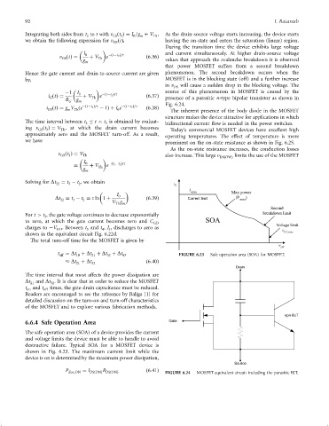
               6.6.4 Safe Operation Area                             Gate
               The safe operation area (SOA) of a device provides the current
               and voltage limits the device must be able to handle to avoid
               destructive failure. Typical SOA for a MOSFET device is
               shown in Fig. 6.23. The maximum current limit while the
               device is on is determined by the maximum power dissipation,
                                                                                              Source
                                             R
                               P diss;ON  ¼ I DSðONÞ DSðONÞ  ð6:41Þ  FIGURE 6.24  MOSFET equivalent circuit including the parasitic BJT.
   101   102   103   104   105   106   107   108   109   110   111