
Page 103 - Rashid, Power Electronics Handbook
P. 103
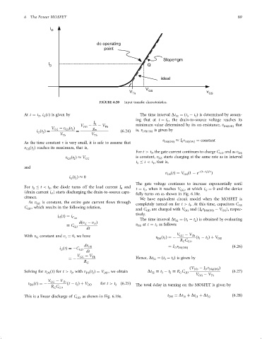
6 The Power MOSFET 89
i
D
dc operating
point
Slope=gm
I
D Q
ideal
V
V GS v
Th GS
FIGURE 6.20 Input transfer characteristics.
At t ¼ t , i ðtÞ is given by The time interval Dt 32 ¼ðt ÿ t Þ is determined by assum-
2
G
3
2
ing that at t ¼ t , the drain-to-source voltage reaches its
3
I 0
V GG ÿ ÿ V Th minimum value determined by its on-resistance, v DSðONÞ that
V GG ÿ v ðt Þ g m
GS 2
i ðt Þ¼ ¼ ð6:24Þ is, v DSðONÞ is given by
G 2
V V
Th Th
v I r ¼ constant
As the time constant t is very small, it is safe to assume that DSðONÞ 0 DSðONÞ
v ðt Þ reaches its maximum, that is,
GS 2
For t > t , the gate current continues to charge C GD and as v DS
3
v ðt Þ V is constant, v GS starts charging at the same rate as in interval
GS 2 GG
t t < t , that is,
1
0
and
v ðtÞ¼ V GG ð1 ÿ e ÿðtÿt 3 Þ=t Þ
GS
i ðt Þ 0
G
2
The gate voltage continues to increase exponentially until
For t t < t , the diode turns off the load current I and t ¼ t , when it reaches V , at which i ¼ 0 and the device
3
0
2
3
GG
(drain current i ) starts discharging the drain-to-source capa- fully turns on as shown in Fig. 6.18e. G
D
citance.
We have equivalent circuit model when the MOSFET is
As v GS is constant, the entire gate current ¯ows through completely turned on for t > t . At this time, capacitors C
C GD , which results in the following relation, 1 GS
and C
GD are charged with V GG and (I r ÿ V GG ), respec-
0 DSðONÞ
tively.
i ðtÞ¼ i
G
C GD
The time interval Dt 32 ¼ðt ÿ t Þ is obtained by evaluating
3
2
dðv ÿ v Þ
D
G
¼ C v DS at t ¼ t as follows:
3
GD
dt
With v constant and v ¼ 0, we have V GG ÿ V Th
G s v ðt Þ¼ ÿ ðt ÿ t Þþ V
DS 3 3 2 DD
R C GD
G
dv DS ¼ I r ð6:26Þ
i ðtÞ¼ ÿC O DSðONÞ
G GD
dt
V GG ÿ V Th
¼ÿ Hence, Dt 32 ¼ðt ÿ t Þ is given by
2
3
R
G
ðV DD ÿ I r Þ
D DSðONÞ
Solving for v ðtÞ for t > t , with v ðt Þ¼ V DD , we obtain Dt 32 ¼ t ÿ t ¼ R C GD ð6:27Þ
G
DS
3
DS 2
2
2
V ÿ V
GG Th
V GG ÿ V Th
v ðtÞ¼ ÿ ðt ÿ t Þþ V DD for t > t 2 ð6:25Þ The total delay in turning on the MOSFET is given by
DS
2
R C GD
G
This is a linear discharge of C GD as shown in Fig. 6.19e. t ON ¼ Dt þ Dt þ Dt 32 ð6:28Þ
10
21