Page 99 - Rashid, Power Electronics Handbook
P. 99

6 The Power MOSFET                                                                                   85

                 a positive constant MOSFET parameter. The term ð1 þ lv Þ  6.6.1 MOSFET Switching Characteristics
                                                                 DS
                 is added to the i equation in order to account for the increase  Because the MOSFET is a majority carrier transport device, it
                              D
                 in i due to the channel-length modulation. Here i is given  is inherently capable of high frequency operation [5–8].
                                                            D
                    D
                 by
                                                                      However, the MOSFET has two limitations:
                                  2                                       1. high input gate capacitances; and
                    i ¼ kðv GS  ÿ V Þ ð1 þ lv Þ  saturation region  ð6:10Þ
                    D
                                         DS
                                Th
                                                                          2. transient=delay due to carrier transport through the
                                                                            drift region.
                 From the de®nition of the r given in Eq. 6.11, it is easy to
                                         0
                 show that the MOSFET output resistance can be expressed as  As stated earlier, the input capacitance consists of two compo-
                 follows:                                             nents: the gate-to-source and gate-to-drain capacitances. The
                                                                      input capacitances can be expressed in terms of the device
                                            1                         junction capacitances by applying the Miller theorem to Fig.
                                   r ¼                         ð6:11Þ
                                    0                                 6.15a. Using the Miller theorem, the total input capacitance
                                       lkðv GS  ÿ V Þ
                                                Th
                                                                      C , seen between the gate-to source, is given by
                                                                       in
                 If we assume that the MOSFET is operating under small signal       C ¼ C þð1 þ g R ÞC             ð6:12Þ
                 condition, that is, the variation in v  on i vs v  is in the         in   gs      m L  gd
                                               GS    D    GS
                 neighborhood of the dc operating point Q at i and v  as
                                                         D      GS
                 shown in Fig. 6.13. As a result, the i current source can be  The frequency responses of the MOSFET circuit are limited by
                                                D
                 represented by the product of the slope g and v  as shown in  the charging and discharging times of C . The Miller effect is
                                                                                                       in
                                                  m     GS
                 Fig. 6.14.                                           inherent in any feedback transistor circuit with resistive load
                                                                      that exhibits a feedback capacitance from the input and
                                                                      output. The objective is to reduce the feedback gate-to-drain
                                                                      resistance. The output capacitance between the drain-to-
                                                                      source C   does not affect the turn-on and turn-off
                   i D                                                        ds
                                                                      MOSFET switching characteristics. Figure 6.16 shows how
                                                                      C gd  and C vary under increased drain-source v Ds  voltage.
                                                            Slope=gm
                                                                              gs
                                                Q                       In power electronics applications, power MOSFET are
                   I D                                                operated at high frequencies in order to reduce the size of
                                                                                          C gd
                                                                             G
                                                                                                                   D
                             V Th
                                                  V GS            v GS
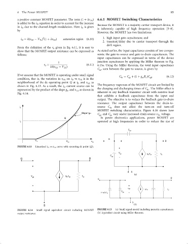
                 FIGURE 6.13  Linearized i D vs v GS curve with operating dc point (Q).
                                                                                    +
                                                                                    V
                                                                                     gs                         r
                                                                                                       g m V gs
                                                                              C                                 O
                                                                               gs   -
                   G                                             D
                           +
                                                                                            S
                                                                                              (a)
                          v                      g v        r
                           gs                     m gs      O                                                         D
                                                                      G
                           -                                                               +
                                                                                          Vgs                       r
                                                                                                     g m V gs
                                                                                      C                             O
                                                                        (1+g m R L )C gd  gs  -
                                                                                             S
                                                                                              (b)
                                   S
                 FIGURE 6.14  Small signal equivalent circuit including MOSFET  FIGURE 6.15  (a) Small signal model including parasitic capacitances.
                 output resistance.                                   (b) Equivalent circuit using Miller theorem.
   94   95   96   97   98   99   100   101   102   103   104