Page 97 - Rashid, Power Electronics Handbook
P. 97

6 The Power MOSFET                                                                                   83

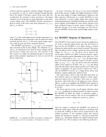
                 of device structure, geometry, and bias voltages. During turn-  In power electronics, the aim is to use power-switching
                 on, capacitors C gd  and C must be charged through the gate,  devices that operate at higher and higher frequencies. Hence,
                                      gs
                 hence, the design of the gate control circuit must take into  the size and weight of output transformers, inductors, and
                 consideration the variation in these capacitances. The largest  ®lter capacitors will decrease. As a result, MOSFETs are now
                 variation occurs in the gate-to-drain capacitance as the drain-  used extensively in power supply design that requires high
                 to-gate voltage varies. The MOSFET parasitic capacitance is  switching frequencies, including switching and resonant mode
                 given in terms of the device data sheet parameters C , C ,  power supplies and brushless dc motor drives. Because of its
                                                             iss
                                                                 oss
                 and C rss  as follows:                               large conduction losses, its power rating is limited to a few
                                                                      kilowatts. Because of its many advantages over BJT devices,
                                    C gd  ¼ C rss                     modern MOSFET devices have received high market accep-
                                    C ¼ C ÿ C  rss                    tance.
                                          iss
                                     gs
                                    C ¼ C oss  ÿ C rss
                                     ds
                 where C rss  is the small-signal reverse transfer capacitance; C iss 6.6 MOSFET Regions of Operation
                 is the small-signal input capacitance with the drain and source
                 terminals shorted; and C oss  is the small-signal output capaci-  Most MOSFET devices used in power electronics applications
                 tance with the gate and source terminals shorted.    are of the n-channel, enhancement type, like that shown in
                   The MOSFET capacitances C , C  and C  are nonlinear
                                            gs  gd     ds             Fig. 6.6a. For the MOSFET to carry drain current, a channel
                 and a function of the dc bias voltage. The variations in C
                                                                  oss  between the drain and the source must be created. This occurs
                 and C   are signi®cant as the drain-to-source voltage and the
                      iss                                             when the gate-to-source voltage exceeds the device threshold
                 gate-to-source voltage each cross zero. The objective of the
                                                                      voltage V . For v GS  > V , the device can be either in the
                                                                              Th
                                                                                           Th
                 drive circuit is to charge and discharge the gate-to-source and
                                                                      triode region, which is also called ‘‘constant resistance'' region,
                 gate-to-drain parasitic capacitances to turn on and off the  or in the saturation region, depending on the value of v .For
                                                                                                                   DS
                 device, respectively.                                given v , with small v DS  (v DS  < v GS  ÿ V ), the device oper-
                                                                                                        Th
                                                                            GS
                             C                                        ates in the triode region (saturation region in the BJT), and for
                               gd                                     larger v  ðv  > v  ÿ V ), the device enters the saturation
                                                                            DS  DS   GS    Th
                                                                      region (active region in the BJT). For v  < V , the device
                                                                                                       GS    Th
                                                                      turns off, with drain current almost equal to zero. Under both
                                                                      regions of operation, the gate current is almost zero. This is
                                                      C
                                                       ds             why the MOSFET is known as a voltage-driven device and,
                                                                      therefore, requires simple gate control circuit.
                                                                        The characteristic curves in Fig. 6.6b show that there are
                                                                      three distinct regions of operation labeled as triode region,
                                                                      saturation region, and cut-off region. When used as a switch-
                             C                                        ing device, only triode and cut-off regions are used, whereas,
                              gs
                                                                      when it is used as an ampli®er, the MOSFET must operate in
                                         (a)
                                                                      the saturation region, which corresponds to the active region
                                          G                           in the BJT.
                       S                                      S         The device operates in the cut-off region (off-state) when
                                                                      v GS  < v , resulting in no induced channel. In order to operate
                                                                            Th
                                             SiO 2                    the MOSFET in either the triode or saturation region, a
                                                                      channel must ®rst be induced. This can be accomplished by
                    n +
                                                            n +       applying gate-to-source voltage that exceeds v , that is,
                                                                                                            Th
                                C gs
                             p
                    C                        C
                     ds                       g     n -                                    v GS  > V Th
                                             d
                                                    n +
                                                                      Once the channel is induced, the MOSFET can operate in
                                                                      either the triode region (when the channel is continuous with
                                                                      no pinch-off, resulting in drain current proportional to the
                                          D                           channel resistance) or the saturation region (the channel
                                          (b)
                                                                      pinches off, resulting in constant I ). The gate-to-drain bias
                                                                                                   D
                 FIGURE 6.9  (a) Equivalent MOSFET representation including junc-  voltage (v GD ) determines whether the induced channel enters
                 tion capacitances; and (b) representation of this physical location.  pinch-off or not. This is subject to the following restriction.
   92   93   94   95   96   97   98   99   100   101   102