
Page 92 - Rashid, Power Electronics Handbook
P. 92
78 I. Batarseh
i
ratio between the change in output voltage DV , with s
o
respect to the change in the input voltage DV . These w +
in
are very important parameters in power electronics v
because the dc input voltage is obtained from a recti®ed sw
line voltage that normally changes by 20%. Therefore, _
any off-line power electronics circuit must have a limited
or speci®ed range of line regulation. If we assume that v sw
the input voltage in Fig. 6.1a,b is changed by 2 V, that is
DV ¼ 2 V, and with R unchanged, the corresponding V off
in
L
change in the output voltage DV is 1 V and 0.55 V,
o
respectively. This is considered very poor line regulation. V on time
Figure 6.1c,d have much better line and load regulations
because the closed-loop control compensates for the line
i sw
and load variations.
I on
6.3 General Switching Characteristics
6.3.1 The Ideal Switch I off time
It is always desirable to have power switches perform as close p(t)
as possible to the ideal case. For a semiconductor device to
operate as an ideal switch, it must possess the following
features:
1. no limit on the amount of current (known as forward time
or reverse current) the device can carry when in the
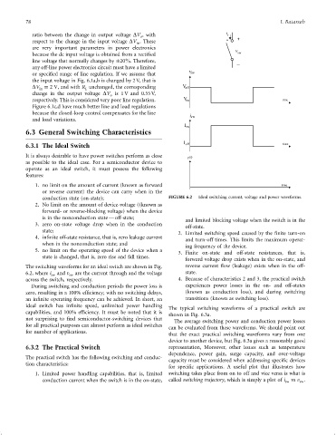
conduction state (on-state); FIGURE 6.2 Ideal switching current, voltage and power waveforms.
2. No limit on the amount of device-voltage ((known as
forward- or reverse-blocking voltage) when the device
is in the nonconduction state Ð off-state;
and limited blocking voltage when the switch is in the
3. zero on-state voltage drop when in the conduction
off-state.
state;
2. Limited switching speed caused by the ®nite turn-on
4. in®nite off-state resistance, that is, zero leakage current
and turn-off times. This limits the maximum operat-
when in the nonconduction state; and
ing frequency of the device.
5. no limit on the operating speed of the device when a
3. Finite on-state and off-state resistances, that is,
state is changed, that is, zero rise and fall times.
forward voltage drop exists when in the on-state, and
The switching waveforms for an ideal switch are shown in Fig. reverse current ¯ow (leakage) exists when in the off-
6.2, where i sw and v sw are the current through and the voltage state.
across the switch, respectively. 4. Because of characteristics 2 and 3, the practical switch
During switching and conduction periods the power loss is experiences power losses in the on- and off-states
zero, resulting in a 100% ef®ciency; with no switching delays, (known as conduction loss), and during switching
an in®nite operating frequency can be achieved. In short, an transitions (known as switching loss).
ideal switch has in®nite speed, unlimited power handling
The typical switching waveforms of a practical switch are
capabilities, and 100% ef®ciency. It must be noted that it is
shown in Fig. 6.3a.
not surprising to ®nd semiconductor-switching devices that
The average switching power and conduction power losses
for all practical purposes can almost perform as ideal switches
can be evaluated from these waveforms. We should point out
for number of applications.
that the exact practical switching waveforms vary from one
device to another device, but Fig. 6.3a gives a reasonably good
6.3.2 The Practical Switch representation, Moreover, other issues such as temperature
dependence, power gain, surge capacity, and over-voltage
The practical switch has the following switching and conduc-
capacity must be considered when addressing speci®c devices
tion characteristics:
for speci®c applications. A useful plot that illustrates how
1. Limited power handling capabilities, that is, limited switching takes place from on to off and vice versa is what is
conduction current when the switch is in the on-state, called switching trajectory, which is simply a plot of i sw vs v .
sw