
Page 91 - Rashid, Power Electronics Handbook
P. 91
6 The Power MOSFET 77
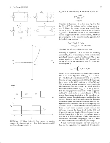
R R P out ¼ 24 W. The ef®ciency of the circuit is given by
+ I +
L
24 W
V v R %
in o R L V in L v o Z ¼
52:8W
_ _
¼ 45:5%
(a) (b)
Transistor dc Regulator: It is clear from Fig. 6.1c that
+ v -
CE for V ¼ 12 V, the collector emitter voltage must by
o
I S I L + 12 V. Hence, the control circuit must provide base
L +
V I B R V in R L v current I to put the transistor in the active mode with
B
in L v o o
Control
V CE 12 V. As the load current is 2 A, then collector
_ _
current is approximately 2 A (assume small I ). The total
B
(d) power dissipated in the transistor can be approximated
(c)
by the following equation:
P diss ¼ V I þ V I
CE C
BE B
V I 12 2 ¼ 24 W
i(A) CE C
Therefore, the ef®ciency of the circuit is 50%.
Switching dc Regulator: Let us consider the switching
circuit of Fig. 6.1d by assuming the switch is ideal and is
periodically turned on and off in Fig. 6.1f. The output
voltage waveform is shown in Fig. 6.1f. Although the
-12V v(V)
output voltage is not constant or pure dc, its average
value is given by
0.01
ð
1 T o
V o;ave ¼ V dt ¼ V D
in
in
T
o
where D is the duty ratio and it equals the ratio of the on-
time to the switching period. For V o;ave ¼ 12 V, we set
D ¼ 0:5, that is, the switch has a duty cycle of 0.5 or 50%.
(e)
Here the average output power is 48 W and the average
input power is also 48 W, resulting in 100% ef®ciency!
This is of course because we assumed that the switch is
switch
ideal. However, if we assume that a BJT switch is used in
forementioned circuit with V ¼ 1 V and I is small,
CE;sat B
then the average power loss across the switch is approxi-
mately 2 W, which creates an overall ef®ciency of 96%. Of
ON OFF ON
course, the switching circuit given in this example is over
t simpli®ed because the switch requires additional driving
0 DT T
circuitry that was not shown, and which also dissipates
some of the power. However, the example illustrates that
v
o
higher ef®ciency can be obtained by switching to a power
V electronic circuit as compared to the ef®ciency obtained
in
from a linear power electronic circuit. Further, the
V
o,ave difference between the linear circuit in Fig. 6.1b and
6.1c and the switched circuit of Fig. 6.1d is that the power
t delivered to the load in the latter case pulsates between
0 DT T
zero and 96 W. If the application calls for constant power
(f)
delivery with little output voltage ripple, then an LC ®lter
FIGURE 6.1 (a) Voltage divider; (b) Zener regulator; (c) transistor must be added to smooth out the output voltage.
regulator; (d) switching circuit; (e) i-v Zener diode characteristics and (f) A ®nal observation is required on what is known as
switching and output waveforms. load and line regulation. Line regulation is de®ned as the