Page 96 - Rashid, Power Electronics Handbook
P. 96

82                                                                                            I. Batarseh

                               GATE   SOURCE                        MOSFET and, unlike the BJT, MOSFET devices do not suffer
                                                                    from second breakdown voltages and sharing current in
                   Metal
                                                                    parallel devices is possible.
                                        SiO
                                           2
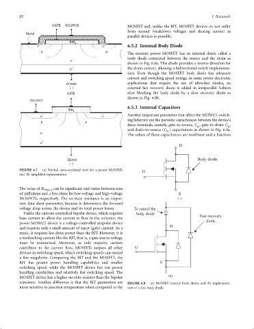
                        n +                             n +         6.5.2 Internal Body Diode
                          P                              P          The modern power MOSFET has an internal diode called a
                                                                    body diode connected between the source and the drain as
                                        n -
                                                                    shown in Fig. 6.8a. This diode provides a reverse direction for
                                        n +                         the drain current, allowing a bidirectional switch implementa-
                                                                    tion. Even though the MOSFET body diode has adequate
                                                                    current and switching speed ratings, in some power electronic
                                                                    applications that require the use of ultra-fast diodes, an
                                      DRAIN
                                        (a)                         external fast recovery diode is added in antiparallel fashion
                                       GATE                         after blocking the body diode by a slow recovery diode as
                                                                    shown in Fig. 6.8b.
                     SOURCE
                                                                    6.5.3 Internal Capacitors
                                       SiO 2
                                                                    Another important parameter that affect the MOSFET switch-
                          n                            n
                                                                    ing behavior are the parasitic capacitances between the device's
                          p                    p
                                                                    three terminals, namely, gate-to-source, C , gate-to-drain C gd
                                                                                                      gs
                                                                    and drain-to-source (C ) capacitances as shown in Fig. 6.9a.
                                                                                       ds
                          n
                                                                    The values of these capacitances are nonlinear and a function
                          n
                                                                                             D
                                                                                                      Body diode
                                       DRAIN
                                        (b)
               FIGURE 6.7  (a) Vertical cross-sectional view for a power MOSFET;  G
               and (b) simpli®ed representation.


               The value of R   can be signi®cant and varies between tens
                           DSðonÞ
               of milliohms and a few ohms for low-voltage and high-voltage                  S
               MOSFETS, respectively. The on-state resistance is an impor-                  (a)
               tant data sheet parameter, because it determines the forward
               voltage drop across the device and its total power losses.
                 Unlike the current-controlled bipolar device, which requires
               base current to allow the current to ¯ow in the collector, the
               power MOSFET device is a voltage-controlled unipolar device
               and requires only a small amount of input (gate) current. As a
               result, it requires less drive power than the BJT. However, it is
               a nonlatching current like the BJT, that is, a gate source voltage
               must be maintained. Moreover, as only majority carriers
               contribute to the current ¯ow, MOSFETs surpass all other
               devices in switching speed, which switching speeds can exceed
               a few megahertz. Comparing the BJT and the MOSFET, the
               BJT has greater power handling capabilities and smaller
               switching speed, while the MOSFET device has less power
               handling capabilities and relatively fast switching speed. The
               MOSFET device has a higher on-state resistor than the bipolar
               transistor. Another difference is that the BJT parameters are  FIGURE 6.8  (a) MOSFET internal body diode; and (b) implementa-
               more sensitive to junction temperature when compared to the  tion of a fast body diode.
   91   92   93   94   95   96   97   98   99   100   101