
Page 107 - Rashid, Power Electronics Handbook
P. 107
6 The Power MOSFET 93
Drain
i
D
r
DS(ON) r D
i
V BD
GD
+ - V +
R + BD Bulk(substrate)
Gate G
i DS V DS
i - i B
G
- - V BS +
Temperature
V
GS
i
BS
FIGURE 6.25 The on-state resistance as a fraction of temperature.
R S
in high-voltage applications. The use of silicon carbide instead I S
of silicon has reduced v DSðOWÞ many fold. Source
As the device technology keeps improving, especially in
terms of improved switch speeds and increased power hand- FIGURE 6.26 Spice L1 MOSFET static model.
ling capabilities, it is expected that the MOSFET will continue
to replace BJTs in all types of power electronics systems. In the saturation (linear) region, where v > V and
GS Th
v > v ÿ V , the drain current is given by
DS GS Th
6.7 MOSFET PSPICE Model I ¼ K P W ðV ÿ V Þ ð1 þ lV Þ ð6:42Þ
2
D
2 L ÿ 2X GS Th DS
j l
The PSPICE simulation package has been used widely by
electrical engineers as an essential software tool for circuit Where K P is the transconductance and X jl is the lateral
design. With the increasing number of devices available in the diffusion.
market place, PSPICE allows for accurate extraction and The threshold voltage V Th is given by
understanding of various device parameters and their varied
q q
effects on the overall design prior to their fabrication. Today's V Th ¼ V T0 þ @ 2f ÿ V BS ÿ 2f p ð6:43Þ
p
PSPICE library is rich with numerous commercial MOSFET
models. This section will give a brief overview of how the
MOSFET model is implemented in PSPICE. A brief overview where, V T0 is the zero-bias threshold voltage; d is the body-
effect parameter; and f is the surface inversion potential.
of the PSPICE modeling of the MOSFET device will be given p
Typically, X L and l 0.
here. ij
The term ð1 þ lV Þ is included in the model as an
DS
empirical connection to model the effect of the output
conductance when the MOSFET is operating in the triode
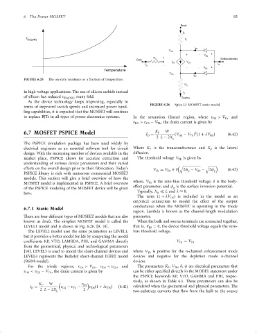
6.7.1 Static Model
region. Lambda is known as the channel-length modulation
There are four different types of MOSFET models that are also parameter.
known as levels. The simplest MOSFET model is called the When the bulk and source terminals are connected together,
LEVEL1 model and is shown in Fig. 6.26. [9, 10]. that is, V BS ¼ 0, the device threshold voltage equals the zero-
The LEVEL2 model uses the same parameters as LEVEL1, bias threshold voltage,
but it provides a better model for Ids by computing the model
coef®cients KP, VTO, LAMBDA, PHI, and GAMMA directly V Tn ¼ V T0
from the geometrical, physical and technological parameters
[10]. LEVEL3 is used to model the short-channel devices and where V T0 is positive for the n-channel enhancement mode
LEVEL4 represents the Berkeley short-channel IGFET model devices and negative for the depletion mode n-channel
(BSIM-model). devices.
For the triode regions, v GS > V , v DS < v , and The parameters K , V , d, f are electrical parameters that
Th
P
GS
T0
v DS < v GS ÿ V , the drain current is given by can be either speci®ed directly in the MODEL statement under
Th
the PSPICE keywords KP, VTO, GAMMA and PHI, respec-
tively, as shown in Table 6.1. These parameters can also be
K P W v DS
i ¼ v GS ÿ v Th ÿ v ð1 þ lv Þ ð6:41Þ calculated when the geometrical and physical parameters. The
D
DS
DS
2 L ÿ 2X 2
j l two-substrate currents that ¯ow from the bulk to the source