
Page 116 - Rashid, Power Electronics Handbook
P. 116
7 Insulated Gate Bipolar Transistor 103
forward blocking state until the open-base breakdown of the
pnp-transistor is reached.
When a positive potential is applied to the gate and exceeds
the threshold voltage required to invert the MOS region under
the gate, an n-channel is formed, which provides a path for
ÿ
electrons to ¯ow into the n -drift region. The pn-junction
ÿ
þ
between the p -substrate and n -drift region is forward-
biased and holes are injected into the drift region. The
electrons in the drift region recombine with these holes to
maintain space-charge neutrality and the remaining holes are
collected at the emitter, causing a vertical current ¯ow between
the emitter and collector. For small values of collector poten-
tial and a gate voltage larger than the threshold voltage, the
on-state characteristics can be de®ned by a wide-base power
BJT. As the current density increases, the injected carrier
density exceeds the low doping of the base region and becomes
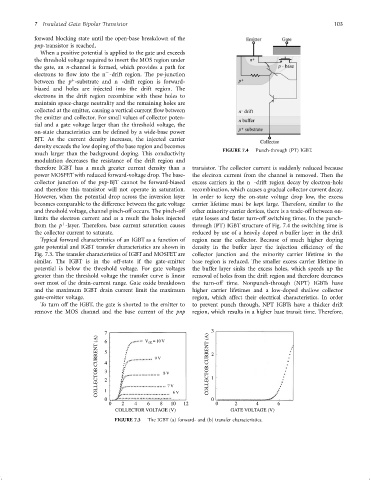
FIGURE 7.4 Punch-through (PT) IGBT.
much larger than the background doping. This conductivity
modulation decreases the resistance of the drift region and
therefore IGBT has a much greater current density than a transistor. The collector current is suddenly reduced because
power MOSFET with reduced forward-voltage drop. The base- the electron current from the channel is removed. Then the
ÿ
collector junction of the pnp-BJT cannot be forward-biased excess carriers in the n -drift region decay by electron-hole
and therefore this transistor will not operate in saturation. recombination, which causes a gradual collector current decay.
However, when the potential drop across the inversion layer In order to keep the on-state voltage drop low, the excess
becomes comparable to the difference between the gate voltage carrier lifetime must be kept large. Therefore, similar to the
and threshold voltage, channel pinch-off occurs. The pinch-off other minority carrier devices, there is a trade-off between on-
limits the electron current and as a result the holes injected state losses and faster turn-off switching times. In the punch-
þ
from the p -layer. Therefore, base current saturation causes through (PT) IGBT structure of Fig. 7.4 the switching time is
the collector current to saturate. reduced by use of a heavily doped n buffer layer in the drift
Typical forward characteristics of an IGBT as a function of region near the collector. Because of much higher doping
gate potential and IGBT transfer characteristics are shown in density in the buffer layer the injection ef®ciency of the
Fig. 7.3. The transfer characteristics of IGBT and MOSFET are collector junction and the minority carrier lifetime in the
similar. The IGBT is in the off-state if the gate-emitter base region is reduced. The smaller excess carrier lifetime in
potential is below the threshold voltage. For gate voltages the buffer layer sinks the excess holes, which speeds up the
greater than the threshold voltage the transfer curve is linear removal of holes from the drift region and therefore decreases
over most of the drain-current range. Gate oxide breakdown the turn-off time. Nonpunch-through (NPT) IGBTs have
and the maximum IGBT drain current limit the maximum higher carrier lifetimes and a low-doped shallow collector
gate-emitter voltage. region, which affect their electrical characteristics. In order
To turn off the IGBT, the gate is shorted to the emitter to to prevent punch through, NPT IGBTs have a thicker drift
remove the MOS channel and the base current of the pnp region, which results in a higher base transit time. Therefore,
7 (A) 3
(A) 6 5 V GE = 10 V 2
COLLECTOR CURRENT 4 3 2 9V 8V COLLECTOR CURRENT 1
0 1 7V 6V 0
0 2 4 6 8 10 12 0 2 4 6
COLLECTOR VOLTAGE (V) GATE VOLTAGE (V)
FIGURE 7.3 The IGBT (a) forward- and (b) transfer characteristics.