
Page 119 - Rashid, Power Electronics Handbook
P. 119
106 S. Abedinpour and K. Shenai
During t load current is transferred from the diode into the the collector voltage reaches the bus voltage, the freewheeling
ri
device and increases to its steady-state value. diode starts to conduct.
ÿ
The gate voltage rise time and IGBT transconductance However, the excess stored charge in the n -drift region
determine the current slope and as a result t . When the during on-state conduction must be removed for the device to
ri
gate-emitter voltage reaches V GEðIonÞ that will support the turn off. The high minority-carrier concentration stored in the
ÿ
steady-state collector current, collector-emitter voltage starts n -drift region supports the collector current after the MOS
to decrease. After this there are two distinct intervals during channel is turned off. Recombination of the minority carriers
IGBT turn-on. In the ®rst interval the collector-to-emitter in the wide-base region gradually decreases the collector
voltage drops rapidly as the gate-drain capacitance C gd of the current and results in a current tail. Because there is no
MOSFET portion of IGBT discharges. At low collector-emitter access to the base of the pnp-transistor, the excess minority
voltage C increases. A ®nite time is required for high-level carriers cannot be removed by reverse-biasing the gate. The t
gd fi2
injection conditions to set in the drift region. The pnp- interval is long because the excess carrier lifetime in this region
transistor portion of IGBT has a slower transition to its on- is normally kept high to reduce the on-state voltage drop.
state than the MOSFET. The gate voltage starts rising again Because the collector-emitter voltage has reached the bus
only after the transistor comes out of its saturation region into voltage in this interval a signi®cant power loss occurs that
the linear region, when complete conductivity modulation increases with frequency. Therefore, the current tail limits the
occurs and the collector-emitter voltage reaches its ®nal on- IGBT operating frequency and there is a trade-off between the
state value. on-state losses and faster switching times. For an on-state
current of I , the magnitude of current tail, and time required
on
for the collector current to decrease to 10% of its on-state
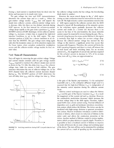
7.4.2 Turn-off Characteristics
value, turn-off (t ) time, are approximated as:
off
Turn-off begins by removing the gate-emitter voltage. Voltage
and current remain constant until the gate voltage reaches I ðtÞ¼ a pnp on ÿðt=t HL Þ ð7:4Þ
I e
c
V GEðIonÞ required to maintain the collector steady-state current
as shown in Fig. 7.9. After this delay time (t dðoffÞ ) the collector t off ¼ t HL lnð10a pnp Þ ð7:5Þ
voltage rises, while the current is held constant. The gate
resistance determines the rate of collector-voltage rise. As the where
MOS channel turns off, collector current decreases sharply
during t . The MOSFET portion of IGBT determines the a ¼ sech l ð7:6Þ
fi1
turn-off delay time t dðoffÞ and the voltage rise time t . When pnp L a
rv
is the gain of the bipolar pnp-transistor, l is the undepleted
basewidth and L is the ambipolar diffusion length and it is
a
V + assumed that the high-level lifetime (t ) is independent of
HL
GG
the minority carrier injection during the collector current
v GE(t) V GE(th) decay.
V GG - t Lifetime control techniques are used to reduce the lifetime
(t ) and the gain of the bipolar transistor (a ). As a result
t HL pnp
t d(off) fi1 the magnitude of the current tail and t off decrease. However,
the conductivity modulation decreases, which increases the
on-state voltage drop in the drift region. Therefore, higher-
t fi2 speed IGBTs have a lower current rating. Thermal diffusion of
I on
impurities such as gold and platinum introduces recombina-
tion centers, which reduce the lifetime. The device can also be
i C(t) irradiated with high-energy electrons to generate recombina-
t
tion centers. Electron irradiation introduces a uniform distri-
bution of defects, which results in reduction of lifetime in the
V entire wafer and affects the conduction properties of the
cc
device. Another method of lifetime control is proton implan-
V CE(on) t tation, which can place defects at a speci®c depth. Therefore, it
v rv
CE(t) is possible to have a localized control of lifetime to improve
t
the trade-off between the on-state voltage and switching speed
FIGURE 7.9 Switching waveforms during IGBT clamped inductive load of the device. The turn-off loss can be minimized by curtailing
turn-off. the current tail as a result of speeding up the recombination