
Page 123 - Rashid, Power Electronics Handbook
P. 123
110 S. Abedinpour and K. Shenai
be introduced in the circuit only after V reaches V ðthÞ as is turn-on switching loss. Turn-off losses can only be reduced
ge
ge
shown in Fig. 7.14, where the collector current rise occurs. The during the Miller effect and MOS turn-off portion of the turn-
voltage tail during turn-on transient is not affected by this off transient, by reducing the gate resistance. However, this
method. In order to prevent shoot-through caused by acci- increases the rate of change of collector voltage, which strongly
dental turn-on of IGBT due to noise, a negative gate voltage is affects the IGBT latching current and RBSOA. During the
required during the off-state. Low gate impedance reduces the turn-off period, the turn-off gate resistor R goff determines the
effect of noise on the gate. maximum rate of collector-voltage change. After the device
During the ®rst slope of the gate voltage turn-on transient turns off, turning on transistor T prevents the spurious turn-
1
the rate of charge supply to the gate determines the collector- on of IGBT by preventing the gate voltage from reaching the
current slope. During the Miller-effect zone of the turn-on threshold voltage.
transient the rate of charge supply to the gate determines the
collector-voltage slope. Therefore, the slope of the collector 7.6.3 Protection
current, which is controlled by the gate resistance, strongly
affects the turn-on power loss. Reduction in switching power Gate-drive circuits can also provide fault protection of IGBT
loss requires low gate resistance. However, the collector- in the circuit. The fault-protection methods used in IGBT
current slope also determines the amplitude of the conducted converters are different from their gate-turn-off thyristor
electromagnetic interference during turn-on switching transi- (GTO) counterparts. In a GTO converter a crowbar is used
ent. Lower electromagnetic interference generation requires for protection and as a result there is no current limiting.
higher values of gate resistance. Therefore, in conventional When the short-circuit is detected the control circuit turns on
gate-drive circuits by selecting an optimum value for R , there all the GTO switches in the converter, which results in opening
g
is a trade-off between lower switching losses and lower of a fuse or circuit breaker on the dc input. Therefore, series
electromagnetic interference generation. di=dt snubbers are required to prevent rapid increase of the
However, the turn-off switching of IGBT depends on the fault current and the snubber inductor has to be rated for large
bipolar characteristics. Carrier lifetime determines the rate at currents in the fault condition. However, IGBT has an impor-
which the minority carriers stored in the drift region recom- tant ability to intrinsically limit the current under overcurrent
bine. The charge removed from the gate during turn-off has and short-circuit fault conditions, and the value of the fault
small in¯uence on minority-carrier recombination. The tail current can be much larger than the nominal IGBT current.
current and di=dt during turn-off, which determine the turn- Thus IGBT has to be turned off rapidly after the fault occurs.
off losses, depend mostly on the amount of stored charge and The magnitude of the fault current depends on the positive-
the minority-carrier lifetime. Therefore, the gate-drive circuit gate bias voltage V . A higher V gg þ is required to reduce
þ
gg
has a minor in¯uence on turn-off losses of the IGBT, while it conduction loss in the device, but this leads to larger fault
affects the turn-on switching losses. currents. In order to decouple the trade-off limitation between
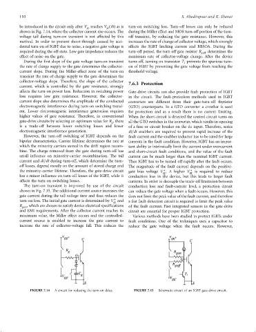
The turn-on transient is improved by use of the circuit conduction loss and fault-current level, a protection circuit
shown in Fig. 7.15. The additional current source increases the can reduce the gate voltage when a fault occurs. However, this
gate current during the tail voltage time and thus reduces the does not limit the peak value of the fault current, and therefore
þ
turn-on loss. The initial gate current is determined by V and
gg a fast fault-detection circuit is required to limit the peak value
R , which are chosen to satisfy device electrical speci®cations
gon of the fault current. Fast integrated sensors in the gate-drive
and EMI requirements. After the collector current reaches its circuit are essential for proper IGBT protection.
maximum value, the Miller effect occurs and the controlled- Various methods have been studied to protect IGBTs under
current source is enabled to increase the gate current to fault conditions. One of the techniques uses a capacitor to
increase the rate of collector-voltage fall. This reduces the reduce the gate voltage when the fault occurs. However,
FIGURE 7.14 A circuit for reducing the turn-on delay. FIGURE 7.15 Schematic circuit of an IGBT gate-drive circuit.