
Page 284 - Rashid, Power Electronics Handbook
P. 284
274 S. Hui and H. Chung
1
S CR1 Lr Lf Io f ¼ p ð15:1cÞ
r
2p L C r
r
i
Lr
Vi Cr Df Cf RL R L
V Cr Vo r ¼ ð15:1dÞ
Z
r
(a) f s
g ¼ ð15:1eÞ
f
r
gate signal
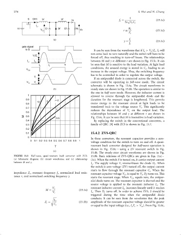
to S It can be seen from the waveforms that if I > V =Z , I will
r
o
i
S
not come back to zero naturally and the switch will have to be
V/Z
i r
forced off, thus resulting in turn-off losses. The relationships
I I between M and g at different r are shown in Fig. 15.5c. It can
Lr O
t 0 t 1 T be seen that M is sensitive to the load variation. At light load
conditions, the unused energy is stored in C , leading to an
V r
DS
increase in the output voltage. Thus, the switching frequency
has to be controlled in order to regulate the output voltage.
V
i
If an antiparallel diode is connected across the switch, the
V V converter will be operating in full-wave mode. The circuit
Cr i
schematic is shown in Fig. 15.6a. The circuit waveforms in
(b) steady state are shown in Fig. 15.6b. The operation is similar to
the one in half-wave mode. However, the inductor current is
1 allowed to reverse through the antiparallel diode and the
0.9 r =2 duration for the resonant stage is lengthened. This permits
10 5
0.8 excess energy in the resonant circuit at light loads to be
transferred back to the voltage source V . This signi®cantly
0.7 i
1 reduces the dependence of V on the output load. The
0.6 o
relationships between M and g at different r are shown in
M 0.5 Fig. 15.6c. It can be seen that M is insensitive to load variation.
0.5
0.4 By replacing the switch in the conventional converters, a
0.3 family of QRC [9] with ZCS is shown in Fig. 15.7.
0.2
0.1 15.4.2 ZVS-QRC
0
In these converters, the resonant capacitor provides a zero-
0 0.1 0.2 0.3 0.4 0.5 0.6 0.7 0.8 0.9 1
voltage condition for the switch to turn on and off. A quasi-
g resonant buck converter designed for half-wave operation is
shown in Fig. 15.8a Ð using a ZV resonant switch in Fig.
(c)
15.4b. The steady-state circuit waveforms are shown in Fig.
FIGURE 15.5 Half-wave, quasi-resonant buck converter with ZCS: 15.8b. Basic relations of ZVS-QRCs are given in Eqs. (1a) –
(a) Schematic diagram; (b) circuit waveforms; and (c) relationship (1e). When the switch S is turned on, it carries output current
between M and g. I . The supply voltage V reverse-biases the diode D . When
o
f
i
the switch is zero-voltage (ZV) turned off, the output current
starts to ¯ow through the resonant capacitor C . When the
r
impedance Z , resonant frequency f , normalized load resis- resonant capacitor voltage V Cr is equal to V , D turns on. This
r
r
f
i
tance r, and normalized switching frequency g.
starts the resonant stage. When V Cr equals zero, the antipar-
allel diode turns on. The resonant capacitor is shorted and the
source voltage is applied to the resonant inductor L . The
r
V o resonant inductor current I increases linearly until it reaches
Lr
M ¼ ð15:1aÞ
V i I . Then D turns off. In order to achieve ZVS, S should be
f
o
triggered during the time when the antiparallel diode
s conducts. It can be seen from the waveforms that the peak
L r
Z ¼ ð15:1bÞ amplitude of the resonant capacitor voltage should be greater
r
C
r or equal to the input voltage (i.e., I Z > V ). From Fig. 15.8c,
o r
in