
Page 288 - Rashid, Power Electronics Handbook
P. 288
278 S. Hui and H. Chung
Buck
Boost
Buck-boost
Cuk
Flyback
Sepic
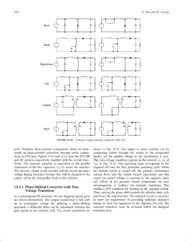
FIGURE 15.10 A family of quasi-resonant converters with ZVS.
path. Therefore, these parasitic components, which are unde- shown in Fig. 15.13. Two upper or lower switches can be
sirable in hard-switched converters, become useful compo- conducting (either through the switch or the antiparallel
nents in ZVS ones. Figures 15.11 and 15.12 show the ZVS HB diode), yet the applied voltage to the transformer is zero.
and FB circuits, respectively, together with the circuit wave- This zero-voltage condition appears in the interval [t ; t ]of
2
1
forms. The resonant capacitor is equivalent to the parallel V pri in Fig. 15.13. This operating stage corresponds to the
connection of the two capacitors (C =2) across the switches. required off time for that particular switching cycle. When
r
The off-state voltage of the switches will not exceed the input the desired switch is turned off, the primary transformer
voltage during resonance because they will be clamped to the current ¯ows into the switch output capacitance and this
supply rail by the antiparallel diode of the switches. causes the switch voltage to resonate to the opposite input
rail. Effects of the parasitic circuit components are used
advantageously to facilitate the resonant transitions. This
15.5.2 Phase-Shifted Converter with Zero
Voltage Transition enables a ZVS condition for turning on the opposite switch.
Thus, varying the phase shift controls the effective duty cycle
In a conventional FB converter, the two diagonal switch pairs and hence the output power. The resonant circuit is necessary
are driven alternatively. The output transformer is fed with to meet the requirement of providing suf®cient inductive
an ac rectangular voltage. By applying a phase-shifting energy to drive the capacitors to the opposite bus rail. The
approach, a deliberate delay can be introduced between the resonant transition must be achieved within the designed
gate signals to the switches [18]. The circuit waveforms are transition time.