
Page 290 - Rashid, Power Electronics Handbook
P. 290
280 S. Hui and H. Chung
L L
S D
V
A
0
S C D
V
B
0
V (a)
PRI
0
Lr
I S C C D
PRI S D
0
(b)
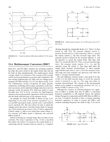
I FIGURE 15.14 Multiresonant switches: (a) ZC-MR switch; and (b) ZV-
D14
0 MR switch.
I
D15
(¯owing through the antiparallel diode of S). Then S is then
0
turned on with ZVS. The resonant inductor current I Lr
t t t 2 t t 3 4 increases linearly and D is still conducting. When I Lr reaches
0 1
f
FIGURE 15.13 Circuit waveforms of the phase-shifted, ZVT FB conver- the output current I , the ®rst resonant stage starts. The
o
ter. resonant circuit is formed by the resonant inductor L and
r
the capacitor C across the output diode. This stage ends
D
when S is turned off with ZVS. Then, a second resonant stage
15.6 Multiresonant Converters (MRC) starts. The resonant circuit consists of L , C , and the
r
D
capacitor across the switch C . This stage ends when the
s
Both ZCS- and ZVS-QRCs optimize the switching condition output diode becomes forward-biased. A third resonant
for either the active switch or the output diode only, but not stage will then start. Here L and C form the resonant circuit.
r
s
for both of them simultaneously. The multiresonant switch This stage ends and completes one operation cycle when the
concept, which is an extension of the concept of the resonant diode C becomes forward-biased.
s
switch, has been developed to overcome such a limitation. The The only difference between mode I and mode II in Fig.
zero-current multiresonant (ZC-MR) and zero-voltage multi- 15.16b is in the third resonant stage, in which the resonant
resonant (ZV-MR) switches [12], [17] are shown in Fig. 15.14. circuit is formed by L and C . This stage ends when D f
r
D
The multiresonant circuits incorporate all major parasitic becomes forward-biased. The concept of the multiresonant
components, including switch output capacitance, diode junc- switch can be applied to conventional converters [19 – 21]. A
tion capacitance, and transformer leakage inductance into the family of MRCs is shown in Fig. 15.17.
resonant circuit. In general, ZVS (half-wave mode) is more Although the variation of switching frequency for regula-
favorable than ZCS in dc-dc converters for high-frequency tion in MRCs is smaller than that of QRCs, a wide-band
operation because the parasitic capacitance of the active switch frequency modulation is still required. Hence, the optimal
and the diode will form part of the resonant circuit. design of magnetic components and the EMI ®lters in MRCs is
An example of a buck ZVS-MRC is shown in Fig. 15.15. not easy. It would be desirable to have a constant switching
Depending on the ratio of the resonant capacitance C =C , frequency operation. In order to operate the MRCs with
D
S
two possible topological modes, namely mode I and mode II, constant switching frequency, the diode in Fig. 15.14 can be
can be operated [20]. The ratio affects the time at which the
voltages across the switch S and the output diode D become D
f
zero. Their waveforms are shown in Fig. 15.16a, b, respectively. S
If diode voltage V falls to zero earlier than switch voltage V , S L r I L f V
D
S
the converter will follow mode I. Otherwise, the converter Lr o I
follows mode II. +V - + I Df o
S
Instead of having one resonant stage, there are three in this V i C D V Df D f C f R L
converter. The mode I operation in Fig. 15.16a is described C S -
®rst. Before the switch S is turned on, the output diode D is
f
conducting and the resonant inductor current I is negative FIGURE 15.15 Buck ZVS-MRC.
Lr